Introduction to LNA: Understanding the Fundamentals
Introduction
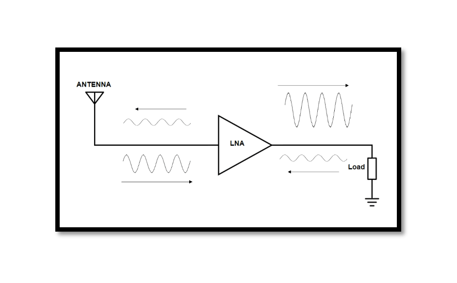
A Low Noise Amplifier (LNA) is a fundamental component within a receiver that plays a crucial role in boosting weak incoming signals while introducing minimal additional noise. It serves as the initial stage in the signal chain of a receiver, amplifying the faint radio frequency (RF) signals captured by the antenna before further processing. The primary function of an LNA is to increase the strength of incoming signals without significantly degrading the signal-to-noise ratio (SNR). Maintaining a low level of added noise is imperative because it ensures that the amplified signal remains distinguishable from the inherent noise within the receiver itself, thereby preserving the integrity of the received information.
LNAs are designed to have high gain, enabling them to amplify weak signals substantially. However, their defining characteristic lies in their low noise figure—a measure of how much additional noise the amplifier introduces to the signal. A low noise figure ensures that the amplified signal retains clarity and integrity, even when operating in conditions where signals are extremely weak.
Ultimately, the LNA acts as the gateway for incoming RF signals, ensuring that even the faintest transmissions are amplified sufficiently for downstream processing while maintaining signal clarity and fidelity. Its critical role in amplifying weak signals with minimal additional noise makes the LNA an indispensable component in modern communication systems and receivers.
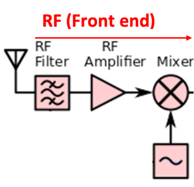
In the RF front end, the Low Noise Amplifier (LNA) holds a critical position, often serving as the initial component that receives and amplifies weak incoming signals captured by the antenna. Its role is paramount in boosting these faint signals while introducing minimal additional noise, thus enhancing the overall sensitivity and performance of the receiver.
Functions in the RF Front End:
- Signal Amplification: The primary function of the LNA in the RF front end is to amplify weak RF signals to levels that are detectable and usable by subsequent stages of the receiver. It significantly increases the signal strength without significantly degrading the signal-to-noise ratio.
- Noise Management: Maintaining a low noise figure is crucial. The LNA is designed to add as little noise as possible to the incoming signal. This ensures that the amplified signal remains discernible from background noise, preserving signal integrity.
- Impedance Matching: The LNA is often designed to match the impedance between the antenna and subsequent receiver stages. This optimization facilitates efficient power transfer from the antenna to the amplifier, minimizing signal loss or distortion.
- Frequency Selectivity: Some LNAs incorporate frequency selectivity, allowing them to amplify signals within a specific frequency band while rejecting others. This feature aids in filtering out unwanted noise or interfering signals.
Placement and Impact:
Placed at the forefront of the receiver, the LNA significantly influences the overall performance of the system. Its ability to amplify weak signals without introducing excessive noise directly affects the receiver’s sensitivity, dynamic range, and ability to detect and process signals in challenging environments.
Challenges and Considerations:
Designing an LNA for the RF front end involves balancing trade-offs between gain, noise figure, power consumption, and linearity. Achieving high gain while maintaining low noise and suitable linearity is a delicate challenge that engineers must address, often resorting to advanced circuit designs and optimization techniques.
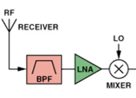
The Low Noise Amplifier (LNA) plays a pivotal role in reducing unwanted noise at the front-end of a radio receiver circuit. Its primary function is to minimize additional noise, a crucial aspect in optimizing the retrieval of the desired signal in subsequent stages of the system. The noise figure (NF) of an LNA is a crucial parameter, and it dominates the overall receiver noise figure. It is calculated as:
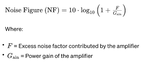
To minimize additional noise, designers focus on choosing low-noise components, appropriate operating points, and circuit topologies that align with the goal of reducing noise while balancing other design objectives like power gain and impedance matching.
The balance between reducing additional noise and achieving other design goals, like maximizing power gain and ensuring proper impedance matching, is critical in the design of LNAs. Achieving this equilibrium ensures optimal performance of the receiver system, enhancing the reception of desired signals while minimizing unwanted noise.
Friss’s formula is a fundamental equation used in understanding the relationship between noise figure, gain, and the number of cascaded stages (amplifiers) in a system. It’s particularly relevant in the context of Low Noise Amplifiers (LNAs) where maintaining a low noise figure is crucial. The formula, attributed to Bernard D. H. Tellegen and Harald T. Friis, describes the total noise figure of a cascaded system:
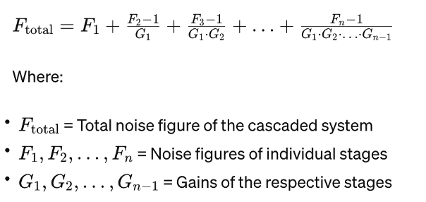
In the context of LNAs, this formula is crucial when multiple amplification stages are cascaded. Each stage adds its own noise contribution to the overall system. The noise figure of the entire cascade is influenced not just by the noise figure of each stage but also by their gains.
For an LNA designer, Friss’s formula serves as a guideline to understand how cascading multiple amplifier stages impacts the overall noise figure of the system. It emphasizes the importance of maintaining low noise figures in individual stages, as a high noise figure in one stage can significantly affect the overall noise performance of the entire system.
When designing LNAs, engineers often aim to use low noise amplification stages to minimize the cumulative noise figure. This may involve optimizing each stage for minimal noise figure while ensuring sufficient gain to meet the overall system requirements. Achieving a low overall noise figure in LNAs is crucial for sensitive receiver applications where signal integrity is paramount, such as in communication systems or sensitive measurement equipment.
Signal Amplification with Minimal Noise:
When an antenna receives RF signals, they often arrive in a weakened state due to various factors such as distance, interference, or environmental conditions. The role of the LNA is to magnify these faint signals to a level that subsequent stages of the receiver can effectively process. However, crucially, the amplification process must not introduce excessive noise that could distort or degrade the signal.
Impedance Matching and Gain:
Additionally, the LNA is engineered to match the impedance between the antenna and subsequent receiver stages, optimizing the transfer of power from the antenna to the amplifier. This impedance matching minimizes signal loss or distortion, allowing the LNA to efficiently extract and amplify the desired signal.
The LNA typically exhibits high gain, meaning it can significantly increase the strength of incoming signals. This high gain allows even weak signals to be boosted substantially, making them more easily detectable and interpretable by the rest of the receiver circuitry.
Example questions related to Low Noise Amplifiers
Here are some example questions involving calculations related to Low Noise Amplifiers (LNAs) and their performance parameters:
1. Noise Figure Calculation:
Question: An LNA has a gain of 20 dB and a noise figure of 2 dB. If the input signal-to-noise ratio (SNR) is 10 dB, what will be the output SNR after passing through this LNA?
Solution: Given: LNA Gain = 20 dB, LNA Noise Figure = 2 dB, Input SNR = 10 dB
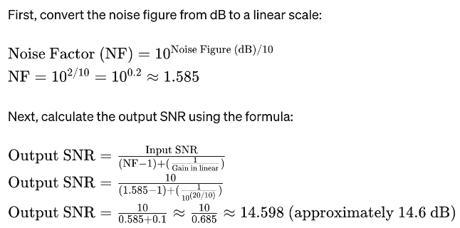
Therefore, the output SNR after passing through the LNA is approximately 14.6 dB.
2. Gain Calculation:
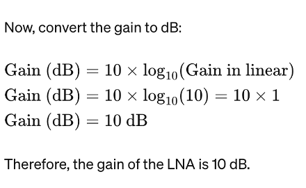
Question: An LNA has an input power of 10 µW and an output power of 100 µW. Calculate the gain of the LNA in dB.
Solution: Given: Input Power = 10 µW, Output Power = 100 µW
The gain (in linear scale) can be calculated using the formula:
Various design processes for LNA
- MMIC (Monolithic Microwave Integrated Circuit) Design:
MMIC LNAs are integrated circuits designed to operate at microwave frequencies. The design process typically involves:
- Specification Definition: Clearly define the performance requirements such as frequency range, gain, noise figure, and power consumption.
- Circuit Topology Selection: Choose the appropriate LNA topology based on the application and specifications. Common topologies include common-source, common-gate, or cascode configurations.
- Device Selection: Select suitable active devices (like HEMTs, HBTs, or CMOS transistors) with low noise and high gain characteristics, compatible with the target frequency range.
- S-Parameter Simulation: Simulate the small-signal S-parameters to analyze and optimize the circuit’s performance using software tools like ADS (Advanced Design System) or Microwave Office.
- Layout and Fabrication: Lay out the circuit design considering microstrip, coplanar waveguide, or other transmission line structures. Fabricate the MMIC using semiconductor fabrication techniques.
- Testing and Characterization: Characterize the fabricated MMIC through measurements to validate its performance against the specified parameters.
- Discrete Component Design:
For lower frequency applications or when flexibility is required, LNAs can also be designed using discrete components like transistors, resistors, and capacitors.
- Transistor Selection: Choose appropriate discrete transistors based on the target frequency range, noise figure, and gain requirements.
- Schematic Design: Create a schematic using discrete components in configurations like common emitter, common base, or others based on the application.
- Simulations: Perform simulations using software like SPICE to optimize the circuit’s performance and ensure it meets the desired specifications.
- Prototype Construction: Assemble the LNA on a prototyping board or PCB based on the finalized schematic.
- Testing and Tuning: Measure the LNA’s performance using network analyzers, spectrum analyzers, and other test equipment. Fine-tune component values for optimal performance.
- PCB-Based LNA Design:
PCB-based LNAs are commonly used for moderate frequency applications and can offer a balance between performance and ease of fabrication.
- Specification Determination: Clearly define the specifications required, including frequency range, gain, noise figure, and power consumption.
- Topology Selection: Choose a suitable LNA topology considering the application requirements and the target frequency range. Common topologies include cascode, common-source, or distributed amplifiers.
- Component Selection: Choose components like transistors, resistors, and capacitors that meet the specifications and can be easily implemented on a PCB.
- PCB Layout: Design the PCB layout considering RF transmission lines, impedance matching networks, and minimizing parasitic elements. Tools like Altium Designer or EagleCAD aid in the layout process.
- Simulations and Prototyping: Use simulation software to validate the design and then create a prototype on the PCB. Verify the performance using network analyzers and spectrum analyzers.
- Fine-Tuning: Adjust component values or layout parameters to optimize performance and ensure the LNA meets the desired specifications.
- RFIC (Silicon/CMOS) LNA Design:
RFIC LNAs, particularly those implemented in silicon/CMOS technologies, are suitable for highly integrated, low-power, and cost-effective applications.
- Technology Selection: Choose the appropriate silicon/CMOS process based on the target frequency range, noise figure requirements, and integration levels.
- Circuit Design: Design the LNA circuit considering the specific characteristics of the chosen technology. CMOS LNAs often utilize common-source or common-gate configurations.
- Layout and Fabrication: Design the layout of the circuit considering the intricacies of the silicon/CMOS process. Fabricate the IC using semiconductor foundry services.
- Post-Fabrication Testing: Characterize the fabricated chip using RF test equipment to measure parameters such as gain, noise figure, linearity, and power consumption.
- Iterative Optimization: Based on testing results, refine the design iteratively to achieve the desired performance metrics.
Silicon/CMOS technology offers the advantage of integration, enabling the inclusion of additional functionality on the same chip. However, PCB-based designs provide flexibility and ease of implementation for specific frequency bands and moderate performance requirements. The choice between these approaches depends on the trade-offs between integration, performance, cost, and manufacturing capabilities for a particular application.
Conclusion
Ultimately, the Low Noise Amplifier plays a crucial role in receivers by boosting weak incoming signals to usable levels while maintaining signal integrity. Its ability to amplify with minimal added noise is paramount in ensuring the receiver’s sensitivity and performance, allowing for the effective extraction of meaningful information from the surrounding electromagnetic spectrum.

Learn more about more topic like this. Browse various RF course on our website and watch the course videos for more detailed understanding https://rahsoft.com/courses/. Rahsoft also provides a certificate on Radio Frequency. All the courses offer step by step approach.

