Basic Steps in Designing a Low-Noise Amplifier (LNA)
Introduction
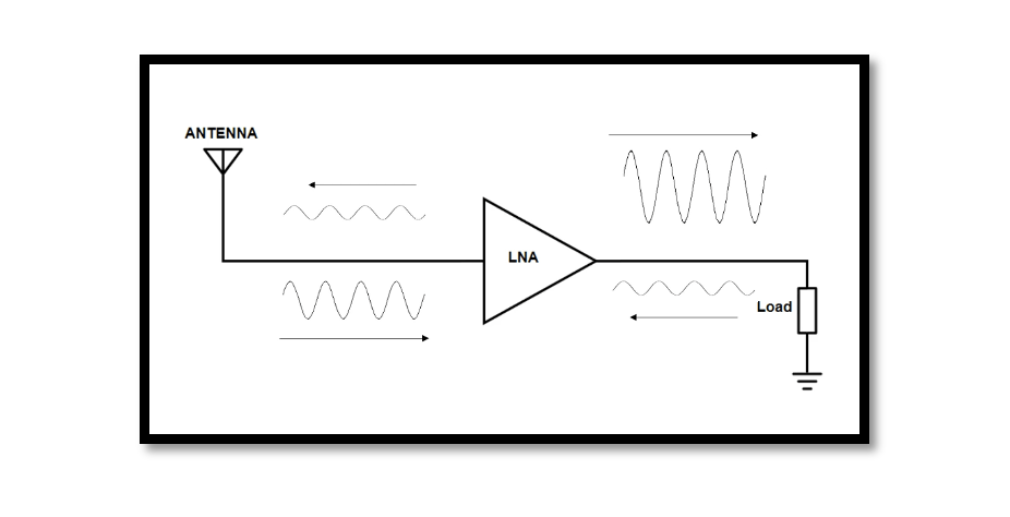
Low-Noise Amplifiers (LNAs) are critical components in radio frequency (RF) systems, essential for amplifying weak signals while adding minimal noise. Designing an LNA requires careful consideration of various parameters to achieve optimal performance. In this guide, we’ll walk through a detailed step-by-step process for designing an LNA, including equations, calculations, and circuit diagrams.
Step 1: Define Specifications
Before diving into the design process, it’s essential to define the specifications for your LNA. This includes parameters such as frequency range, gain, noise figure, input/output impedance, and power consumption. These specifications will guide the design process and ensure that the LNA meets the required performance criteria.
- Frequency range: Define the frequency band over which the LNA will operate.
- Gain: Determine the desired gain to amplify weak signals to a usable level.
- Noise figure: Specify the maximum allowable noise figure to maintain signal integrity.
- Input/output impedance: Define the input and output impedance to match with other components in the system.
- Power consumption: Set limits on power consumption to ensure efficiency.
ADS Process:
- Launch ADS and create a new project.
- Define the specifications for your LNA, including frequency range, gain, noise figure, input/output impedance, and power consumption.
Step 2: Choose the Transistor
Selecting the appropriate transistor is crucial for LNA design. Common choices include field-effect transistors (FETs) such as GaAs MESFETs or CMOS transistors. The transistor should have low noise, high gain, and appropriate frequency characteristics for the application.
Select a transistor based on:
- Technology: Choose between FETs (such as GaAs MESFETs) or CMOS transistors based on performance requirements and fabrication constraints.
- Noise characteristics: Look for transistors with low noise figure and adequate gain for the desired frequency range.
Biasing requirements: Consider the biasing scheme required by the chosen transistor.
ADS Process:
- Use the built-in component libraries in ADS to select an appropriate transistor model (e.g., GaAs MESFET or CMOS).
- Import the transistor model into your project.
Step 3: Calculate Noise Figure (NF)
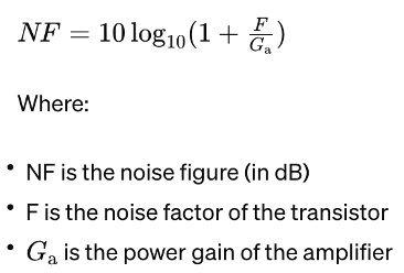
The noise figure quantifies how much the amplifier degrades the signal-to-noise ratio (SNR) of the input signal. The noise figure (NF) of an LNA can be calculated using the following equation:
Step 4: Determine Gain (G)
The gain of the LNA is another critical parameter and is typically specified in decibels (dB). The gain can be calculated using the following equation:

Step 5: Select Biasing Scheme
Proper biasing is essential for optimal transistor performance. Common biasing schemes include voltage biasing and current biasing. The biasing scheme chosen should ensure stability and linearity while minimizing power consumption.
Choose a biasing scheme (e.g., voltage biasing, current biasing) based on:
- Transistor requirements: Ensure stable operation and linearity of the transistor.
- Power consumption: Minimize power consumption while maintaining desired performance.
ADS Process:
- Create a new schematic layout.
- Place the selected transistor model on the schematic.
- Add biasing components such as resistors or voltage sources to bias the transistor properly.
Step 6: Design Matching Networks
Matching networks are used to match the impedance of the transistor to the input and output impedances of the LNA. These networks are typically implemented using passive components such as capacitors and inductors. The design of matching networks involves impedance matching techniques to maximize power transfer and minimize reflections.
Design matching networks to match the impedance of the transistor to the input and output impedances of the LNA. Consider:
- Input and output impedances: Match with source and load impedances for maximum power transfer.
- Frequency response: Design networks to maintain desired frequency response and minimize reflections.
ADS Process:
- Design input and output matching networks using ADS’s built-in tools or by manually placing components such as capacitors and inductors.
- Use the Smith chart and impedance matching techniques to ensure impedance matching between the transistor and the source/load.
Step 7: Simulate and Optimize
Once the LNA circuit is designed, it’s essential to simulate its performance using software tools such as SPICE. Simulations can help identify potential issues and optimize the design for better performance. Parameters such as gain, noise figure, and stability should be verified through simulations.
Use simulation tools such as SPICE to:
- Verify performance: Simulate gain, noise figure, stability, and other parameters to ensure they meet specifications.
- Optimize design: Adjust component values and configurations to improve performance and meet design goals.
ADS Process:
- Set up simulations to analyze the LNA’s performance.
- Configure AC analysis to sweep the frequency range of interest.
- Perform S-parameter and noise simulations to analyze gain, noise figure, and stability.
- Use optimization tools in ADS to fine-tune component values and optimize LNA performance.
- Optimize for maximum gain while meeting noise figure requirements.
- Adjust component values in matching networks to achieve optimal impedance matching.
Step 8: Fabricate and Test
After simulation and optimization, the LNA circuit can be fabricated using appropriate technologies such as printed circuit board (PCB) or integrated circuit (IC) fabrication. Once fabricated, the LNA should be tested using RF test equipment to verify its performance against the specifications.
Fabricate the LNA circuit and test it using RF test equipment:
- Verify performance: Measure gain, noise figure, and other parameters to validate against specifications.
- Tune if necessary: Fine-tune component values or configurations to optimize performance if deviations are observed.
By following these detailed steps, designers can effectively design and optimize Low-Noise Amplifiers to meet the requirements of various RF applications.
ADS Process:
- Create a new layout design for the LNA circuit.
- Place components on the layout according to the schematic design.
- Route interconnects and transmission lines carefully to minimize parasitic effects and ensure proper signal integrity.
- Use ADS’s EM simulation capabilities to analyze the layout’s electromagnetic behavior.
- Perform EM simulations to verify transmission line characteristics, parasitic effects, and impedance matching.
- Adjust layout if necessary based on simulation results.
- Perform final simulations to verify LNA performance against specifications.
- Export the design for fabrication if satisfied with simulation results.
- Fabricate the LNA circuit and test it using RF test equipment to validate performance in real-world conditions.
Conclusion
Designing a Low-Noise Amplifier demands a systematic approach, integrating theoretical principles with practical implementation. Leveraging Advanced Design System (ADS), designers can navigate the intricate intricacies of LNA design, from defining specifications to fabricating and testing the finalized circuit. By following this comprehensive guide, designers can craft LNAs tailored to meet the demands of diverse RF applications with precision and efficiency.

Learn more about this topic by taking the complete course ‘Microwave Amplifier and Low Noise Amplifier (LNA) Design Theory and Principles online course – RAHRF526’. Watch the course videos for more detailed understanding. Also checkout other courses on RF system and IC design on https://rahsoft.com/courses/. Rahsoft also provides a certificate on Radio Frequency. All the courses offer step by step approach.
Tag:LNA, Low Noise Amplifier

