Crucial Role of Matching Networks in LNA Design
Impedance matching between the antenna and the Low Noise Amplifier (LNA) is crucial for optimizing the performance of RF systems. The inherent impedance of antennas, typically around 50 ohms, needs to be efficiently transferred to the input impedance of the LNA for maximum power transfer and minimal signal loss.
Directly altering the design of the LNA to match the antenna impedance can be impractical and may compromise the LNA’s performance. The input impedance of the LNA often includes complex values due to components like transistors and capacitances, making it challenging to directly match to a 50-ohm load impedance.
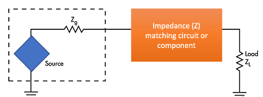
To address this challenge, matching networks come into play. These networks, typically implemented using passive components like inductors and capacitors, are placed between the antenna and the LNA to achieve impedance transformation while preserving the original LNA design. The key concept in designing matching networks is to transform the complex conjugate of the source impedance (Zs*) to the desired load impedance (Zl). In this case, the complex conjugate of the antenna’s output impedance is matched to the input impedance of the LNA. One common approach is to use L-section or pi-section matching networks, which offer flexibility in impedance transformation while maintaining simplicity in design. These networks allow engineers to achieve the desired impedance matching by appropriately selecting the values of the reactive components.
Mastering Matching Circuits in ADS: A Step-by-Step Guide
Matching circuits are particularly critical in the design of Low Noise Amplifiers (LNAs), where signal integrity and noise performance are paramount. LNAs are commonly used in RF and microwave receivers to amplify weak signals while minimizing additional noise contribution. Effective impedance matching at the input and output of the LNA is essential to ensure maximum power transfer, minimal signal distortion, and optimal noise figure.
In the context of LNA design, the matching circuit at the input stage serves to match the relatively low impedance of the antenna or the preceding stage to the input impedance of the LNA. Similarly, at the output stage, the matching circuit matches the output impedance of the LNA to the impedance of the following stage or load. Achieving proper impedance matching at both stages helps to minimize signal reflections, maximize power transfer, and improve overall system performance.
Introduction
Matching circuits play a crucial role in optimizing signal transfer between various components within an electronic circuit. Whether you’re designing a radio frequency (RF) amplifier, a microwave system, or any other high-frequency application, achieving impedance matching is key to maximizing power transfer and minimizing signal loss. In this guide, we’ll delve into the intricacies of designing matching circuits using Advanced Design System (ADS), a powerful tool widely used in the field of RF and microwave engineering.

Step 1: Define System Parameters Before diving into the design process, it’s essential to have a clear understanding of your system’s parameters. This includes knowing the source impedance (Zg) and the load impedance (ZL). These values will serve as the starting point for your matching circuit design. Additionally, identify the frequency range of operation and any specific performance requirements for your circuit.
Step 2: Launch ADS and Set Up the Workspace Launch ADS and create a new workspace for your matching circuit design. Define the project name and select the appropriate design template based on your requirements. Ensure that the frequency range and other simulation settings are correctly configured to match your system parameters.
Step 3: Insert Schematic Components Begin by inserting the necessary components into the schematic layout. This typically includes the source, Zg, the impedance matching circuit or component, and the load, ZL. You can find these components in the ADS component library or create custom components if needed. Connect these components appropriately to form a complete circuit diagram.
Step 4: Choose Matching Topology Select the appropriate matching topology based on your system requirements and available components. Common matching circuits include L-section matching networks, pi-section matching networks, T-section matching networks, and more. Each topology offers advantages and disadvantages in terms of complexity, bandwidth, and performance. Choose the one that best suits your design goals.
Step 5: Design Matching Circuit Components Design the matching circuit components to achieve the desired impedance transformation between the source and the load. This involves calculating the component values such as inductors, capacitors, or transmission lines based on the selected matching topology and desired impedance transformation ratios. ADS provides various design tools and optimization techniques to streamline this process and ensure accurate results.
Step 6: Simulate and Optimize Simulate the designed matching circuit to evaluate its performance and verify its impedance matching capabilities. Use ADS simulation features to analyze key parameters such as return loss, insertion loss, and bandwidth. If necessary, utilize optimization algorithms to fine-tune the component values for optimal matching performance. Iteratively refine the design until the desired specifications are met.
Step 7: Validate with Practical Measurements Once satisfied with the simulation results, validate the matching circuit design through practical measurements. Fabricate the circuit prototype and use network analyzers or other measurement instruments to characterize its performance in real-world conditions. Compare the measured results with the simulation data to ensure consistency and identify any discrepancies that may require further adjustments.
Step 8: Documentation and Reporting Document the design process, including all simulation setups, optimization steps, and measurement results. Prepare a comprehensive report detailing the design methodology, performance evaluation, and any insights gained during the process. This documentation serves as a valuable reference for future projects and facilitates knowledge sharing within your team or organization.
Advanced Design System (ADS) provides powerful simulation capabilities for optimizing LNA matching circuits while considering both impedance matching and noise performance. ADS allows engineers to simulate various matching topologies, optimize component values, and analyze key parameters such as noise figure, gain, and stability. By leveraging ADS’s optimization algorithms, engineers can efficiently fine-tune the matching circuit design to achieve the desired performance metrics.
In summary, matching circuits play a crucial role in LNA design by ensuring proper impedance matching and noise performance at the input and output stages. By leveraging tools like ADS, engineers can effectively design and optimize matching circuits to maximize the performance of LNAs in RF and microwave receiver systems.
Conclusion
Designing matching circuits in ADS requires a systematic approach, starting from defining system parameters to validating the final design through simulations and practical measurements. By following the step-by-step guide outlined above, you can effectively design matching circuits that optimize signal transfer and enhance the overall performance of your RF and microwave systems. With practice and experience, mastering matching circuits in ADS will become a valuable skill in your toolbox as an RF engineer.

Learn more about this topic by taking the complete course ‘Microwave Amplifier and Low Noise Amplifier (LNA) Design Theory and Principles online course – RAHRF526’. Watch the course videos for more detailed understanding. Also checkout other courses on RF system and IC design on https://rahsoft.com/courses/. Rahsoft also provides a certificate on Radio Frequency. All the courses offer step by step approach.


