The Importance of Matching Networks in Amplifier Design
Amplifier Model
Matching Networks play a crucial role in optimizing the performance of amplifiers by ensuring maximum power transfer between different components. In the context of an antenna and Low Noise Amplifier (LNA) setup, impedance matching becomes particularly important. The input impedance of the LNA (Zl) and the output impedance of the antenna (Zs) need to be properly matched for efficient power transfer. Typically, the output impedance of antennas is around 50 ohms. Achieving maximum power transfer requires the load impedance (Zl) to be matched to the complex conjugate of the source impedance (Zs*). However, directly altering the design of the LNA to achieve this match is often impractical, as it would necessitate significant redesign and potentially compromise performance. For instance, the design of the LNA may involve components such as transistors and capacitances, resulting in an input impedance that includes imaginary reactance values. Matching these impedances directly to the 50-ohm load impedance is not feasible. Therefore, the challenge lies in delivering maximum power without modifying the LNA’s design or changing its input impedance.
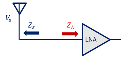
One effective solution to this challenge is the utilization of matching networks. These networks serve as intermediary components between the antenna and the LNA, facilitating optimal impedance matching without necessitating alterations to existing circuit designs. By incorporating a matching network, the load impedance presented to the LNA can be transformed into the complex conjugate of the source impedance, thereby meeting the requirement for maximum power transfer (Zl = Zs*). This approach ensures efficient power delivery from the antenna to the LNA, enhancing overall system performance without the need for extensive redesign efforts.

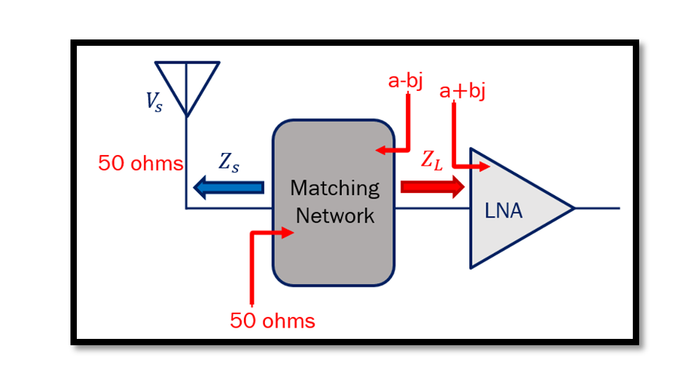
In the architecture depicted above, the matching network serves as a vital intermediary between different components within the RF system. It essentially partitions the circuit into two distinct segments: the source and the load. This matching circuitry can be strategically placed between various blocks of RF systems, such as between the antenna and LNA or between the filter and LNA, depending on the system requirements. Its primary function is to transform the impedance at its input to the conjugate of the source impedance (Zs*). By designing the matching circuit in such a manner that its input impedance matches the conjugate of the source impedance, maximum power transfer can be achieved within the system.
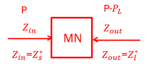
Upon proper design and implementation, the matching network ensures that all power entering it is efficiently transmitted to the load without significant losses. At the output of the matching network, power transmission is ideally lossless, with all power directed towards the load. However, it’s essential to acknowledge that achieving absolute losslessness is practically unattainable, and there will always be some degree of acceptable power loss (PL). Therefore, while striving for optimal performance, engineers must consider and mitigate these losses to the best extent possible.
When designing matching networks, it’s imperative to utilize reactive elements such as inductors (L) and capacitors (C). These elements are chosen for their ability to manipulate impedance without absorbing average power. Unlike resistors, which dissipate power in the form of heat, reactive elements play a pivotal role in impedance transformation while maintaining efficient power transfer within the system. By judiciously selecting and configuring these reactive components, engineers can tailor matching networks to suit specific impedance requirements, thereby optimizing the performance of RF systems.
Understanding Input and Output Equivalent Circuits in Matching Networks
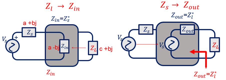
In the context of matching networks, it’s crucial to examine both the input and output equivalent circuits to ensure effective impedance transformation. The input impedance (Zin) of the matching circuit is designed to mirror the complex conjugate of the source impedance (Zs*). For instance, if the source impedance is represented as Zs = a + bj, then the corresponding input impedance becomes Zin = a – bj. The goal of this design approach is to seamlessly transition the impedance from the output to the input of the matching circuit.
Conversely, in the output equivalent circuit, the matching network is engineered to yield an output impedance (Zout) that matches the complex conjugate of the load impedance (Zl*). By achieving this transformation, the matching network ensures efficient power transfer from the source to the load.
Consider the scenario of an antenna and a Low Noise Amplifier (LNA) interconnected via a matching network. To facilitate maximum power transfer, the impedance characteristics must be carefully managed. If the antenna exhibits an output impedance of 50 ohms, the input impedance (Zin) of the matching circuit should ideally match this value. Simultaneously, the input impedance (Zl) to the LNA may be represented as a + bj, while the output impedance of the matching circuit corresponds to a – bj.
In summary, the objective of designing a matching circuit is to achieve impedance transformations where Zin equals Zs* and Zout equals Zl*. This ensures seamless power transmission from Zin to Zout while minimizing acceptable losses (PL). Through meticulous design and configuration, engineers strive to optimize the performance of matching networks within RF systems.

Learn more about this topic by taking the complete course ‘Microwave Amplifier and Low Noise Amplifier (LNA) Design Theory and Principles online course – RAHRF526’. Watch the course videos for more detailed understanding. Also checkout other courses on RF system and IC design on https://rahsoft.com/courses/. Rahsoft also provides a certificate on Radio Frequency. All the courses offer step by step approach.
Tag:Amplifier, LNA, Matching network

