Understanding Input Referred Noise in Circuits
Noise in circuits
In the previous section on Different types of noise in RF devices, we discussed that every component within the circuit contributes to some kind of noise. The device noise added to the external noise degrades the SNR at the output. This noise is generated by the components used to design the blocks, like resistor, transistor & non-ideal inductor. The Power Spectral Density (PSD) of a signal describes the power present in a signal as a function of frequency, and PSD also shows the variations in strength as a function of frequency. An amplifier circuit contains components like resistors, transistors and these components generate noise.

What is input-referred noise?
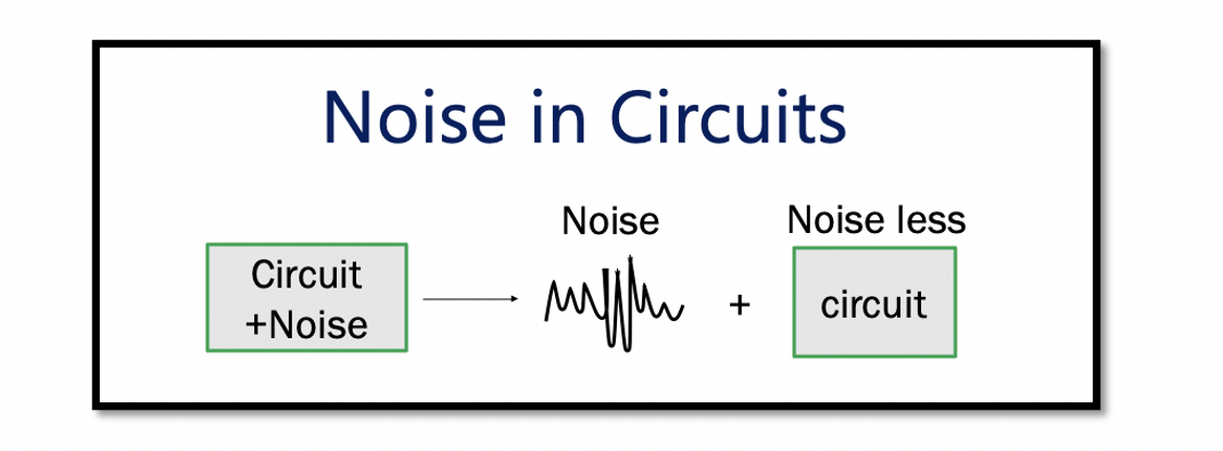
To analyse noisy circuits more efficiently, the concept of an input-referred noise model can be used. In this kind of model, if we imagine we have a circuit and associated noise. On separating the noise from the circuit, we get a pure circuit without any noise, therefore the circuit is noiseless. This is the concept of input-referred noise.
Pulling out the noise from the output of the circuit and making it as an input of the circuit, the whole system remains noisy; however, the difference is we get two parts. These two parts are; the noise source part at the input and the noiseless circuit, as shown below.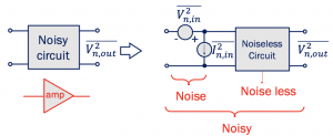
How to find input-referred noise?

Step 1: Short all voltage sources and open all current sources. If we have a noise source inside the amplifier, then it is required to get rid of all the voltage sources inside the circuit while doing a noise analysis. In this case, Vs and VDD. Step by step diagram for the circuits is shown below for better understanding.
Step 2: Insert the source noise one by one in the circuit. In this example, the circuit has many different noise sources. Suppose this amplifier has one resistor and one transistor. The three noise sources would be a resistor, transistor, and Rs inside the amplifier.
Start one by one, and don’t pull out all the noise sources together. This step means assuming other sources are not noisy; consider it 0. Take one source simultaneously, like Rs, as a thermal noise source, and then find out the output response for this noise source which is the 3rd step.
Step 3: Finding out the output response for the selected noise source (repeat for each noise source). If PSD for Rs is VR2 we want to see what is the response of the output VROUT.
The steps are repeated for each individual noise source, each time assuming other noise sources to be 0.
Step 4: Sum all noise output responses using superposition theory. There are different kinds of noise (current and voltage). Bringing all these noise sources to the output will have some gain. The total noise at the output is the integration of all the noise sources. Calculate output noise for all the components.
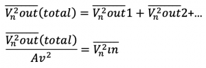
For the last step, we need to find the input-referred noise. We have the output noise, but this has to be the input noise (concept of input-referred noise). For doing that, divide the total output by the gain of the system. The result is input-referred noise.

Learn more about this topic by taking the complete course ‘’RF Design Theory and Principles – RAHRF201’’.
Watch the course videos for more detailed understanding. Also checkout other courses on RF system and IC design on https://rahsoft.com/courses/
Rahsoft also provides a certificate on Radio Frequency. All the courses offer step by step approach.

