Examples to Understand Input Referred Noise and Noise Figure
How to find Input Referred Noise in the given circuit?
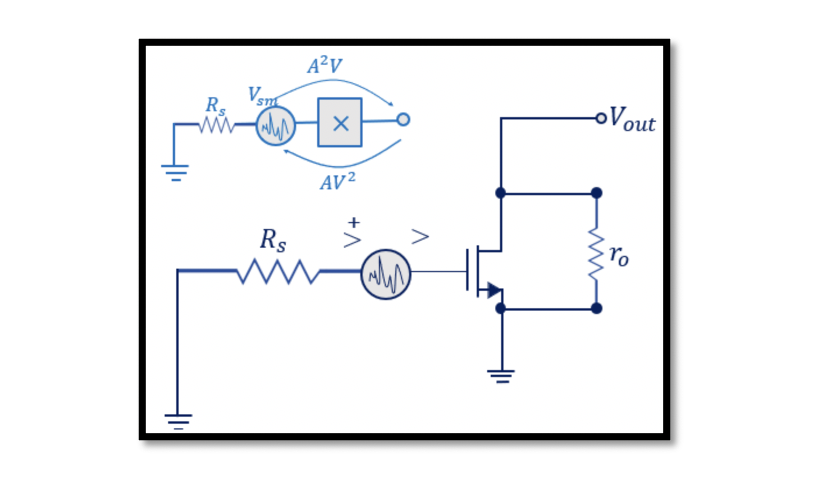
Read about input-referred noise. In the below circuit diagram, Vs is the source, and Rs is the resistance of the source. R0 represents the short channel. IB is the bias current source, and the resistance of this is infinity; hence, this resistance can be neglected compared to the output resistance of the transistor.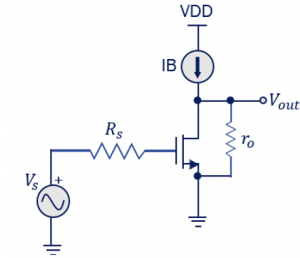
Step 1: Cancel out the effect of the sources. We have to make the source voltage to 0. Vs=0 -> and ID another source should be 0 as well, so ID->open. ID is between transistor and VDD, so we are not concerned about VDD if the ID is open.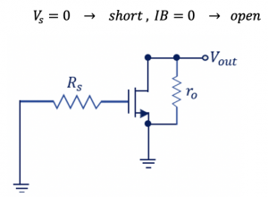
Step 2: The noise sources are from the transistor, and we assume that we have only channel noise, ignoring the flicker noise and gate-induced noise. Another noise source is Rs which is thermal noise.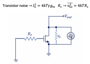
Step 3: Find the output voltage of this circuit. Firstly cancelling the noise effect of the resistor, and we proceed with the transistor. We need to find the effect of transistor noise at the output.
If we notice the transistor model as shown below, Vgs is 0 for this circuit, so the value of gmVgs is 0, so left out are two components, ro, and In2. To find out the Vout in terms of ro and In2 we can write as: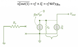
Step 4: We have voltage source noise for Rs, so how to find the effect of this noise at the output. Assume this circuit a common source amplifier. This noise source is at the gate of the transistor. To move this noise source to the output, we multiply it with the gain of the transistor. Therefore, it can be written as: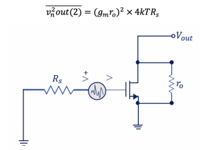
Step 5: So to find the total voltage multiply by gain:

This equation gives the input-referred noise that is calculated for the given circuit. Where 4kTRs is the noise of Rs, and it appears at the input. So when you have source resistance, noise at the input of your block can be written directly. Noise coming from the source that is the source resistance noise always appears at the output as input-referred noise.
4kTY/gm is coming from the channel noise, and to decrease this noise, gm has to be increased. Hence, we say power has a relationship with noise; it is inversely proportional to noise. Increasing the power will decrease the noise. Input referred noise will be decreased in this circuit if we bias this transistor with high power. These are some important points to remember while designing RF circuits.
How to find the Noise Figure in the circuit?
Imagine this system is noisy, and it’s connected to a source, and Rs is the resistance of the source in the system.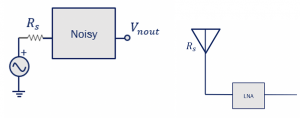
So this system in real-world can be represented as shown below, with an antenna with resistance Rs and let the noisy system represent the LNA which employs the components like transistors and resistors that generate noise. Finding out the NF for this system, we need to find the SNRin and SNRout.
SNRin is the signal’s power ratio at the input (Psig, in) to the power of noise at the input (Pnoi, in). The noisy system has input resistance or input impedance. So the system can be modelled as shown where we need to find the voltage Vin at the node. Vin is the voltage division between Rs and Rin. So power at the input can be found as:
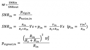
We have only one noise source at the input of this block. So when we are going to find the noise. As we know from the previous section, there is a resistance at the source to be a thermal noise. But this time, we have PSD of noise as this is thermal noise. Power of noise at the input (Pnoi, in) can be found as:
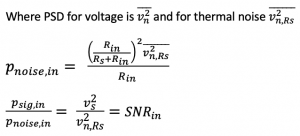
Note: Most of the time, Rs is equal to Rin, which is 50 ohms.
Now we need to find SNRout for this given system. SNRout is power of signal at the output to power of noise at the output:

Before we proceed, we need to separate the noise from the noisy circuit. As discussed before, we can show a noisy system as a noisy and noiseless block in the input-referred noise section. On separating the noise from the circuit, we get a pure circuit without any noise, and the circuit becomes noiseless. This is the concept of input-referred noise.
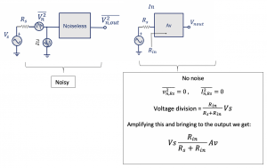
To find the signal’s power at the output (Psignal, out) and we know when we are trying to find the signal, we have to cancel out the effect of noise. So we say no noise. Let the voltage gain of the system be Av, and Rin is the input impedance of this block.

We have three kinds of independent noise sources for this circuit, and we need to find the effect of these noise sources at the output: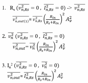
We have three different sources, and we can see the effect at the output. Now to combine them and write them as a signal to noise ratio at the output, we get: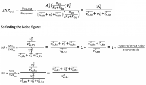
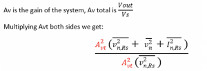
Total noise at the output will be PSD/gain total multiplied by one by 4kTRs due to thermal noise, so we get the NF.

Rs can be the noise coming from other blocks. Move all the noise source to output and combine the effect at the output (Vn,out) and then find the total gain of the system.


