Understanding the Concept of RLC Matching Circuits
Why matching circuits are needed?
As we know that in RF systems maximum power delivery is the main objective while designing a circuit and to maximise the power delivery with minimum loss, matching networks are created. Read understanding the need of matching networks.
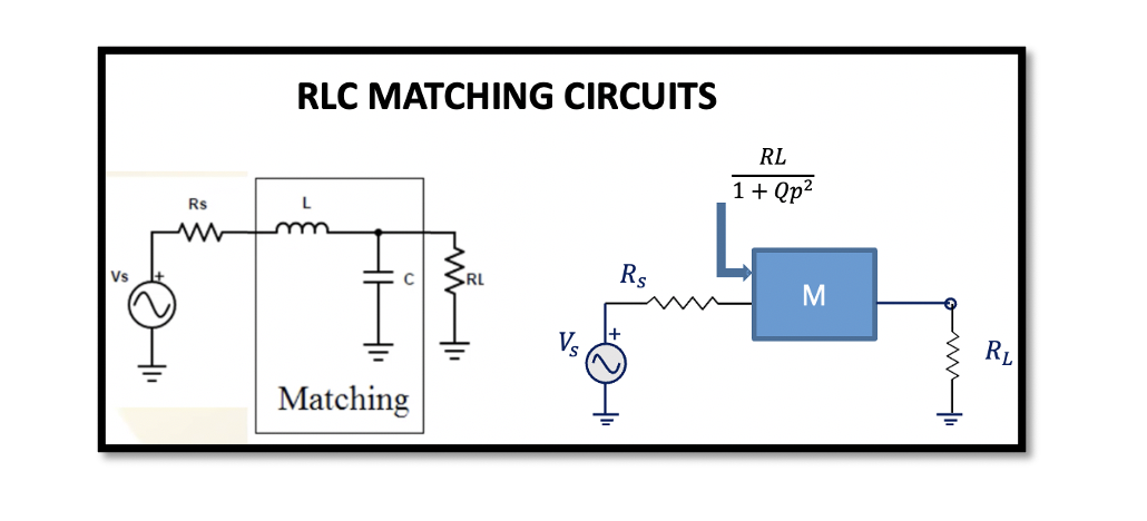
The main goal of RLC circuit is designing matching circuits. We have a circuit as shown below with Rs as the source impedance and RL as the load impedance. So in order to have maximum power transfer in a circuit RL should be equal to Rs. As we read before in the maximum power concept that to have maximum power transfer in a circuit, the load impedance Zl must be matched to the complex conjugate of the source impedance Zs*.
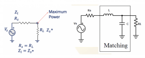
Assuming that we do not have equal resistances in this circuit therefore, we would need matching circuit which has only reactive elements like L & C. With this matching circuit maximum power can be delivered to RL. The input of the matching circuit should be Rs as Zin should be equal to conjugate of source impedance Zs* however, we assume that we have only real part therefore Rin=Rs
In previous section input impedance using Quality Factor and Resonance in RLC circuits we calculated the input impedance Zin using RLC circuit which is equal to:

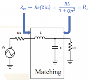
Here, Qp means quality factor of C and RL. In order to make this circuit as matching, Zin should be equal to Rs. So we have to design LC in order to reach this matching.
We know the load resistance RL and the working frequency w. The only thing we have to change is C. When we change C we also have to change L. In previous section input impedance using Quality Factor and Resonance in RLC circuits we read that in method 2 when Qp2 was not higher than 1, L was calculated as: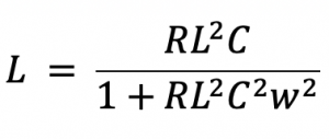

Now that we can calculate w, RL & C, L can be calculated using the above equation. L & equivalent C in this parallel circuit are in resonance so the only thing left here is Rs. We have to say that the imaginary part of Zin is equal to 0. Designing this matching circuit the output resistance can be transferred to input of the matching circuit by dividing it with 1+ Qp2. In summary, we have designed L & C so, the equivalent matching circuit can be shown as: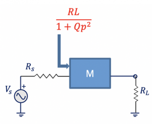

Learn more about this topic by taking the complete course ‘’RF Design Theory and Principles – RAHRF201’’.
Watch the course videos for more detailed understanding. Also checkout other courses on RF system and IC design on https://rahsoft.com/courses/
Rahsoft also provides a certificate on Radio Frequency. All the courses offer step by step approach.

