Introduction to Phase-Locked Loops (PLLs)
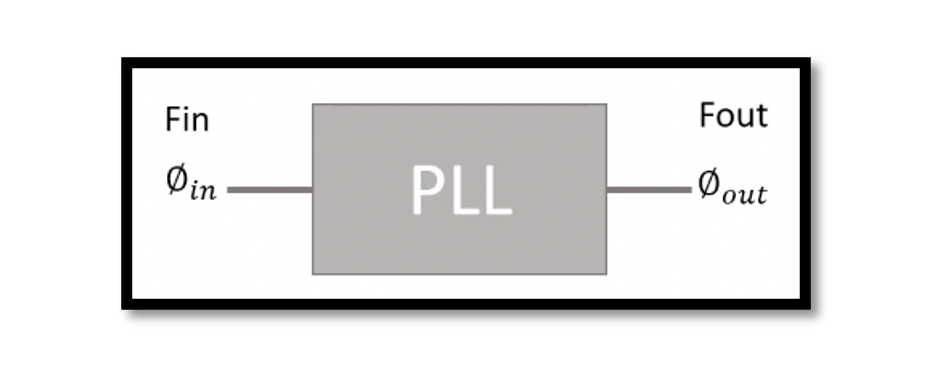
A Phase-Locked Loop (PLL) is a control system that generates an output signal whose phase is related to the phase of an input signal. It is a fundamental building block in many electronic systems, particularly in communications and signal processing.
What is a PLL?
At its core, a PLL synchronizes the phase and frequency of its output signal with an input signal. This synchronization is crucial for various applications such as signal demodulation, clock generation, and frequency synthesis.
The objective of the PLL is to adjust the VCO’s output so that the phase difference between the input and output signals is constant, thereby locking the frequencies.
How PLL Works
- Phase Detection: The PD measures the phase difference between the input signal and the VCO’s output signal. The output of the PD is a voltage proportional to this phase difference.
- Filtering: The LPF smoothens the PD output, removing high-frequency noise and ripple, and produces a control voltage.
- Oscillation Control: The control voltage adjusts the VCO’s frequency and phase, aligning it with the input signal.
Simplified PLL Example
In its simplest form, a PLL is a negative feedback loop consisting of a VCO and a PD. Here’s how it works:
- The PD compares the input phase (ϕin) with the output phase (ϕout) and produces a voltage proportional to the phase difference.
- This voltage controls the VCO, adjusting its frequency and phase.
- If ϕout−ϕin is constant, then the frequencies are equal, and the PLL is locked.
However, if the control voltage has ripple, it modulates the VCO and can produce sidebands. Therefore, it’s crucial to have a well-designed low-pass filter to minimize these effects.
Take our entry level course (Below) for free using coupon code RAHRF101BLOG
RF Fundamentals, Basic Concepts and Components – RAHRF101
For limited time take an additional 10% off of all our courses using coupon code RFCERT10
Rahsoft RF Certificate and courses
Common Problems in PLLs
1. Lock Range and Capture Range
- Lock Range: The range of input frequencies over which the PLL can maintain lock once it is locked.
- Capture Range: The range of input frequencies over which the PLL can achieve lock from an unlocked state.
Problem: If the input frequency falls outside the capture range, the PLL may fail to lock. Additionally, if the input frequency drifts outside the lock range, the PLL can lose lock.
Solution: Design the PLL with adequate lock and capture ranges for the specific application. This can involve choosing appropriate components and adjusting the loop filter parameters.
2. Lock Time
Problem: The time it takes for the PLL to achieve lock from an unlocked state can be critical in applications where quick synchronization is required. Long lock times can delay the system’s response.
Solution: Optimize the loop filter design to balance between lock time and stability. Faster lock times generally require a higher loop bandwidth, but this can reduce noise performance.
3. Phase Noise and Jitter
Phase Noise: Random fluctuations in the phase of the signal, which appear as spectral spreading in the frequency domain.
Jitter: Time-domain variation of the signal’s phase, often caused by phase noise.
Problem: High phase noise and jitter can degrade system performance, particularly in communication systems where signal integrity is crucial. For example, in digital systems, jitter can cause timing errors, leading to data corruption.
Solution: Use low-noise components, improve power supply filtering, and carefully design the loop filter to minimize noise contribution. Sometimes, additional jitter-cleaning circuits might be necessary.
4. Reference Spurious Signals
Problem: Spurious signals or spurs are unwanted frequencies that appear at the output of the PLL due to imperfections in the reference oscillator or phase detector.
Solution: Use high-quality, low-noise reference oscillators and design the loop filter to suppress spurious signals. Ensure that the phase detector and VCO are free from nonlinearities that could generate spurs.
5. Power Supply Noise
Problem: Noise on the power supply can couple into the PLL circuitry, causing frequency modulation of the VCO and increasing phase noise and jitter.
Solution: Implement good power supply decoupling and filtering techniques. Use low-noise power supply regulators and layout practices that minimize power supply noise coupling.
6. Temperature Stability
Problem: Temperature variations can affect the components of the PLL, especially the VCO, causing frequency drift and potentially losing lock.
Solution: Use temperature-compensated components and design the PLL to operate within the expected temperature range of the application. Implementing temperature compensation circuits can also help maintain stability.
7. Component Variations
Problem: Variations in the components due to manufacturing tolerances can affect the PLL’s performance, leading to issues with lock range, noise, and stability.
Solution: Select high-precision components and, if necessary, implement calibration routines to compensate for component variations. Design the PLL with margins to tolerate component tolerances.
8. Nonlinearities
Problem: Nonlinear behavior in the VCO or phase detector can cause distortion and generate harmonics, leading to unwanted spectral components.
Solution: Use linear phase detectors and VCOs with a wide linear range. Ensure the loop filter is designed to handle the expected operating conditions without causing nonlinear behavior.
9. Control Voltage Ripple
Problem: Ripple on the control voltage can modulate the VCO, causing sidebands around the carrier frequency.
Solution: Design the loop filter to minimize ripple and ensure it has sufficient attenuation at the ripple frequency. Good power supply filtering and decoupling can also help.
Conclusion
PLLs are essential components in modern electronics, enabling precise control of signal phase and frequency. Understanding the basic operation and applications of PLLs provides a foundation for exploring more advanced topics in communication systems and signal processing.

Learn more about this topic by taking the complete course ‘Phase Lock Loop System Design Theory and Principles RAHRF469’. Watch the course videos for more detailed understanding. Also checkout other courses on RF system and IC design on https://rahsoft.com/courses/. Rahsoft also provides a certificate on Radio Frequency. All the courses offer step by step approach.
Tag:Phase Locked Loop, PLL


