Understanding the Operation of a Phase-Locked Loop (PLL)
Introduction
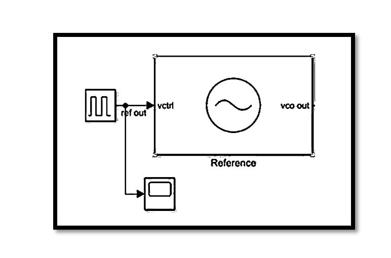
A Phase-Locked Loop (PLL) is an essential component in modern electronic systems, used extensively in applications such as telecommunications, signal processing, and clock generation. This blog post will delve into the operation of a PLL using a simple Simulink model, provide insights into how simulations can be conducted, and illustrate the waveforms involved in the process.
Simple PLL Simulink Model
The basic architecture of a PLL consists of the following components:
- Reference Oscillator (Ref Osc): Generates a reference signal.
- Phase Detector (PD): Compares the phase of the reference signal with the phase of the output signal from the Voltage-Controlled Oscillator (VCO).
- Loop Filter: Filters the signal from the PD to produce a control voltage.
- Voltage-Controlled Oscillator (VCO): Generates an output signal whose frequency is controlled by the input voltage.
Components Explained:
- Reference Oscillator (Ref Osc): Provides a stable frequency reference.
- XOR Phase Detector (PD): Measures the phase difference between the reference signal and the VCO output.
- Convert: A signal conditioning block.
- Butter Filter: Represents the loop filter, which smooths out the PD output.
- VCO: Adjusts its frequency based on the control voltage.
Take our entry level course (Below) for free using coupon code RAHRF101BLOG
RF Fundamentals, Basic Concepts and Components – RAHRF101
For limited time take an additional 10% off of all our courses using coupon code RFCERT10
Rahsoft RF Certificate and courses
How to Perform Simulations
Simulations help in understanding the dynamic behavior of PLLs. Here, we examine the effect of changing the reference oscillator frequency from 𝜔1ω1 to 𝜔2ω2.
Simulation Setup
- Initial Frequency 𝜔1: 1 GHz
- Final Frequency 𝜔2: 1.1 GHz
The simulation shows how the VCO output frequency adjusts to match the new reference frequency.
Key Equations:
The VCO frequency 𝑓𝑜 is given by:
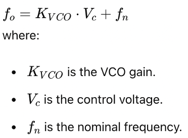
When the reference frequency increases from 𝜔1 to 𝜔2, the control voltage 𝑉𝑐 adjusts to match this change, leading to:

Analyzing the Waveforms
The waveforms below depict the behavior of the PLL during the frequency transition:
Description:
- Ref: The reference signal waveform, changing from 𝜔1 to 𝜔2.
- VCO: The VCO output, adjusting to match the reference frequency.
- PD Output: The output of the phase detector, indicating the phase difference.
- VCO Control Voltage: The control voltage that regulates the VCO frequency.
Observations:
- Initially, the VCO output frequency 𝐹𝑣𝑐𝑜 matches the reference frequency 𝐹𝑟𝑒𝑓=𝜔1.
- When the reference frequency increases to 𝜔2, the phase detector detects a phase difference, and the loop filter adjusts the control voltage.
- The control voltage increases, causing the VCO frequency to rise until it locks onto the new reference frequency 𝜔2.
Key Takeaways:
- The PLL uses feedback to maintain a stable and accurate output frequency.
- Changes in the reference frequency are tracked by the VCO through adjustments in the control voltage.
- Simulation tools like Simulink provide valuable insights into the dynamic performance of PLLs, facilitating better design and analysis.
Conclusion
A PLL effectively synchronizes the output frequency of the VCO with a reference frequency. Through simulations, we observe how the system dynamically adjusts to changes in the reference frequency, ensuring the VCO output remains locked to the desired frequency. Understanding the waveforms and the behavior of each component is crucial for designing and optimizing PLL systems in various applications.

Learn more about this topic by taking the complete course ‘Phase Lock Loop System Design Theory and Principles RAHRF469’. Watch the course videos for more detailed understanding. Also checkout other courses on RF system and IC design on https://rahsoft.com/courses/. Rahsoft also provides a certificate on Radio Frequency. All the courses offer step by step approach.
Tag:Phase Locked Loop, PLL

