Power Amplifiers: A Detailed Exploration of the General Circuit
Power amplifiers are crucial components in many electronic systems, particularly in communication devices, where they boost the power of a signal for transmission. This blog post dives deep into the general circuit of power amplifiers, breaking down each component and explaining their roles and interactions. We’ll cover the schematic, matching networks, transistor biasing, power characteristics, and efficiency.
Schematic Overview
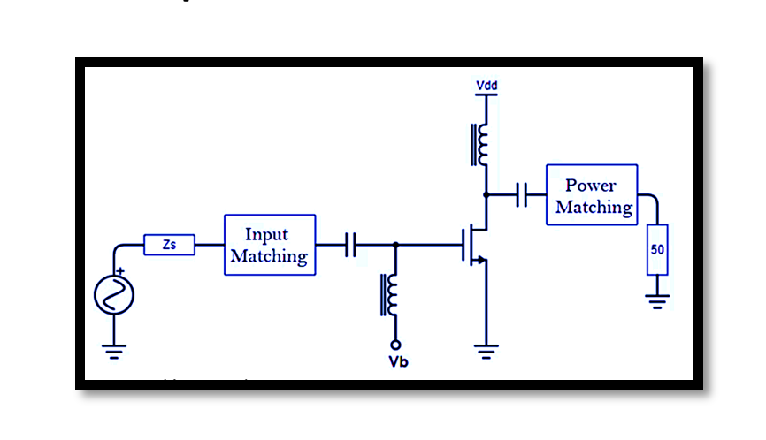
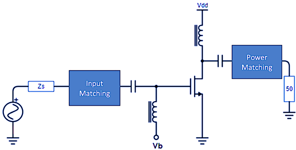
The power amplifier circuit comprises several key sections:
- Source: Provides the input signal, characterized by its source impedance ZS=RS+jXS.
- Input Matching Network: Ensures impedance matching between the source and the amplifier to maximize power transfer.
- Transistor (Active Device): Often a MOSFET, it amplifies the input signal.
- Biasing Network: Provides the necessary DC bias to set the transistor’s operating point.
- Output Matching Network: Matches the transistor’s output impedance to the load impedance, typically 50 ohms in RF applications.
Input Matching
The input matching network plays a crucial role in optimizing the power transfer from the source to the amplifier. The goal is to transform the source impedance ZS into the desired input impedance Zin of the transistor. This is achieved by using reactive components (inductors and capacitors) to cancel out any reactive parts of the impedances.

By designing the input matching network to satisfy the condition ZS=Zin∗ where Zin∗ is the complex conjugate of Zin, maximum power transfer is ensured.
Transistor Biasing
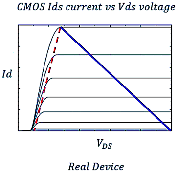
Proper biasing of the transistor is essential to maintain it in the desired region of its operation. For a MOSFET, the gate bias Vb sets the operating point, ensuring the transistor operates in the saturation region for linear amplification. The key characteristics of the transistor’s operation can be observed in the ID vs. VDS curve.

where VGS is the gate-source voltage, and Vth is the threshold voltage. The load line on this characteristic curve is crucial as it shows the range of operation for the amplifier. The slope of the load line is determined by the load resistance and intersects the ID vs. VDS curve at different points, defining the operating region.
Power Matching
The output matching network is designed to maximize the power delivered to the load. This network transforms the output impedance of the transistor Zout to match the load impedance ZL, typically 50 ohms.

The optimal load impedance Zopt is selected to achieve maximum power output and efficiency, which might not necessarily be the conjugate of Zout.
CMOS Ids vs. Vds Characteristics
The current-voltage characteristics of the MOSFET provide insight into the operation of the amplifier. The ID vs. VDS graph shows the relationship between the drain current and the drain-source voltage, with a distinct linear and saturation region. The load line on this graph helps identify the operating points of the amplifier. The intersection of the load line with the transistor’s characteristic curves determines the actual operating points, which should ideally lie in the saturation region for linear amplification.
Power Dissipation and Generated Power
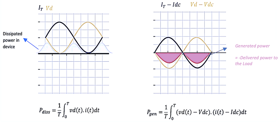
Understanding power dissipation and generated power is vital for designing efficient amplifiers. Power dissipation in the device can be calculated using:

where vDS(t) and iD(t) are the instantaneous drain-source voltage and drain current, respectively. The generated power, which is the power delivered to the load, is given by:

where VDC and IDC are the DC components of the drain-source voltage and drain current.
Efficiency
The efficiency μ of the power amplifier is a critical metric, representing the ratio of the power delivered to the load to the total power consumed. It is given by:

Where Pout is the power delivered to the load, and Pdiss is the power dissipated in the device.
Take our entry level course (Below) for free using coupon code RAHRF101BLOG
RF Fundamentals, Basic Concepts and Components – RAHRF101
For limited time take an additional 10% off of all our courses using coupon code RFCERT10
Rahsoft RF Certificate and courses
Conclusion
Designing a power amplifier involves careful consideration of several factors, including input and output matching, transistor biasing, and power dissipation. By understanding and optimizing these aspects, one can design amplifiers that deliver maximum power to the load with high efficiency. This detailed exploration of the power amplifier circuit provides a comprehensive guide to understanding and designing effective power amplifiers for various applications.

Learn more about this topic by taking the complete course ‘Linear RF Power Amplifier (PA) Design Theory and Principles online course – RAHRF562’. Watch the course videos for more detailed understanding. Also checkout other courses on RF system and IC design on https://rahsoft.com/courses/. Rahsoft also provides a certificate on Radio Frequency. All the courses offer step by step approach.

