A Comprehensive Guide to Class A Amplifiers
Class A amplifiers are fundamental components in the world of electronics, especially in high-frequency applications like RF and audio amplification. Known for their linearity and fidelity, Class A amplifiers have a unique place in amplifier design. This blog provides an in-depth look into Class A amplifiers, covering their structure, device package, power gain, compression point, parasitics, and a detailed example design process.
Structure of Class A Amplifiers
Class A amplifiers are characterized by their operation where the output transistor conducts for the entire cycle of the input signal. This continuous operation ensures that the amplifier remains in the linear region, providing high-fidelity output with minimal distortion.
Key Components:
- Transistor: The main amplifying device, typically a Bipolar Junction Transistor (BJT) or Field-Effect Transistor (FET).
- Biasing Network: Sets the operating point of the transistor to ensure it remains in the active region throughout the input signal cycle.
- Load Resistor (RL): Converts the amplified current signal into a voltage signal.
- Coupling and Bypass Capacitors: Block DC components and allow AC signals to pass, ensuring stable operation and preventing DC bias shifts.
Device Package Structure
The device package in a Class A amplifier, especially for high-frequency applications, plays a crucial role in performance. The package includes the transistor and necessary connections, encapsulated to protect and integrate with external circuits.
Typical Elements in a Device Package:
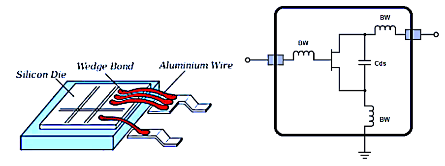
- Silicon Die: The actual semiconductor where the transistor resides.
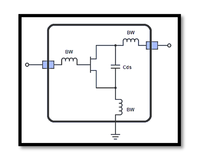
- Bond Wires: Connect the die to the package leads, introducing parasitic inductance.
- Encapsulation: Protects the silicon die and bond wires from environmental factors and mechanical damage.
Power Gain and Compression Point
Power Gain (GP): Power gain is the ratio of the output power to the input power. It is a crucial parameter in amplifier design, defining how much the amplifier boosts the signal.

1 dB Compression Point (P_1dB): The 1 dB compression point indicates the output power level at which the gain drops by 1 dB from its linear value. This point is significant as it marks the maximum output power the amplifier can deliver while maintaining linearity.
Device Package and Parasitics
Parasitics are unwanted reactive components (inductance, capacitance) that arise from the physical construction of the device package. At high frequencies, these parasitics can significantly affect the performance.
Common Parasitics:
- Bond Wire Inductance (L_BW): Inductance introduced by the bond wires connecting the die to the package leads.
- Parasitic Capacitance (C_ds): Capacitance between the drain and source (or collector and emitter) due to the proximity of conducting paths within the package.
To mitigate these effects, careful layout design and the use of appropriate circuit models during simulation are necessary.
Example Design Steps for a Class A Power Amplifier
Let’s provide a detailed example design of a Class A power amplifier using a GaAs MESFET operating at 1.8 GHz, aiming for a typical output power of 1 Watt.
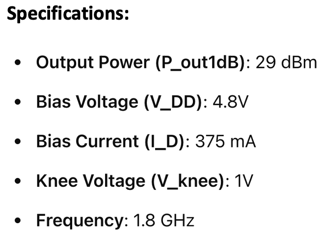
Step 1: Determine the Operating Point Set the DC bias point using the provided specifications.
Step 2: Calculate Optimal Load Resistance (Ropt)

Step 3: Design the Bias Network Design a bias network to establish the desired operating point. This network includes resistors and capacitors to stabilize the operating point without affecting the AC performance.
Step 4: Impedance Matching Use matching networks to transform the load impedance to the calculated Ropt. Impedance matching ensures maximum power transfer and minimizes reflections.
Step 5: Include Parasitics Incorporate parasitic elements (L_BW, C_ds) into the circuit model. Use simulation tools like ADS (Advanced Design System) to account for these elements and predict performance accurately.
Step 6: Simulate and Optimize Simulate the complete amplifier circuit, including the transistor, matching networks, and parasitic elements. Verify key performance metrics such as gain, output power, and linearity. Adjust component values and layout to optimize performance.
Take our entry level course (Below) for free using coupon code RAHRF101BLOG
RF Fundamentals, Basic Concepts and Components – RAHRF101
For limited time take an additional 10% off of all our courses using coupon code RFCERT10
Rahsoft RF Certificate and courses
Conclusion
Class A amplifiers are essential for applications requiring high linearity and fidelity. Understanding their structure, power gain, compression point, and the impact of parasitics is crucial for successful design. By following a systematic design approach, including careful biasing, impedance matching, and parasitic management, engineers can develop efficient and reliable Class A amplifiers for high-frequency applications. This detailed guide provides a comprehensive framework for designing and optimizing Class A power amplifiers, ensuring robust performance in RF and other demanding environments.

Learn more about this topic by taking the complete course ‘Linear RF Power Amplifier (PA) Design Theory and Principles online course – RAHRF562’. Watch the course videos for more detailed understanding. Also checkout other courses on RF system and IC design on https://rahsoft.com/courses/. Rahsoft also provides a certificate on Radio Frequency. All the courses offer step by step approach.
Tag:Class A Amplifier, PA

