PLL Design – Initial Values
In this blog, we will delve into the initial design considerations for a Phase-Locked Loop (PLL), focusing on determining initial values based on system requirements and design principles. The images provided outline the key steps and equations used in the process. Let’s break down each component and equation in detail.
System Bandwidth (w3dB)
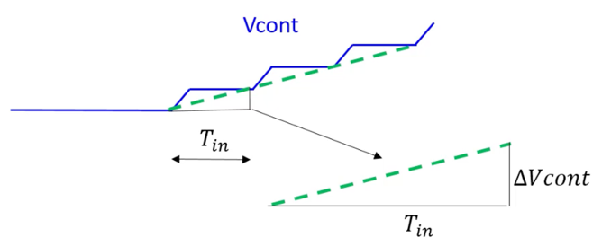
The system bandwidth of a PLL is a critical parameter that defines the frequency range over which the PLL can effectively track the input signal. The initial design requires determining the w3dB , which is the -3dB bandwidth of the loop.
Continuous Approximation Validity
Continuous approximation is valid when the PLL operates much slower than the input signal. This ensures that the PLL can track the input signal without significant phase errors. If the PLL is too fast compared to the input signal, the continuous approximation breaks down, leading to inaccurate tracking.
Rule of Thumb for Bandwidth
A practical rule of thumb for setting the initial bandwidth is:

where wref is the reference frequency.
Example Calculation
Given:
- Reference frequency (fref) = 20 MHz
- Division ratio (M) = 120
We aim to find the initial values for the damping factor (ζ), natural frequency (wn), charge pump current (ICP), and loop filter capacitance (C1).
Step-by-Step Calculation:
- Damping Factor (ζ): For simplicity, we start with a damping factor (ζ) of 1. ζ=1
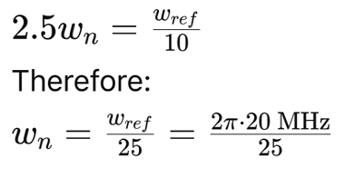
- System Bandwidth (w3dB): The bandwidth (w3dB) is related to the natural frequency (wn) by: w3dB=2.5wn
- Natural Frequency (wn): Using the rule of thumb:
4. Charge Pump Current (ICP) and Loop Filter Capacitance (C1): The equation governing the loop filter design is:

5. Calculating C1: Rearranging the equation for C1:

With KVCO being the VCO gain, which needs to be known or assumed based on the specific design requirements.
From the above calculations, assuming the VCO gain KVCO and substituting the known values: C1=13 pF
PLL Block Diagram
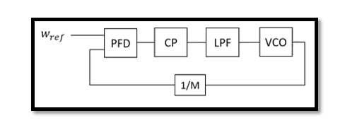
The PLL block diagram consists of the following components:
- Phase Frequency Detector (PFD)
- Charge Pump (CP)
- Low Pass Filter (LPF)
- Voltage-Controlled Oscillator (VCO)
- Divider (1/M)
The reference frequency wref feeds into the PFD, which compares the phase of the input signal with the feedback signal from the VCO divided by M. The charge pump generates a current proportional to the phase difference, which is filtered by the LPF to control the VCO frequency. The VCO output is then divided and fed back to the PFD, completing the loop.
Take our entry level course (Below) for free using coupon code RAHRF101BLOG
RF Fundamentals, Basic Concepts and Components – RAHRF101
For limited time take an additional 10% off of all our courses using coupon code RFCERT10
Rahsoft RF Certificate and courses
Conclusion
The initial design of a PLL involves determining key parameters such as the damping factor, natural frequency, charge pump current, and loop filter capacitance. Using a reference frequency and the division ratio, these values can be calculated to set the PLL’s initial performance metrics. This detailed approach ensures a robust starting point for further optimization and fine-tuning in specific applications.

Learn more about this topic by taking the complete course ‘Phase Lock Loop System Design Theory and Principles RAHRF469’. Watch the course videos for more detailed understanding. Also checkout other courses on RF system and IC design on https://rahsoft.com/courses/. Rahsoft also provides a certificate on Radio Frequency. All the courses offer step by step approach.
Tag:PLL, PLL design, System bandwidth

