Brief Review of the Structure of MOS Transistors
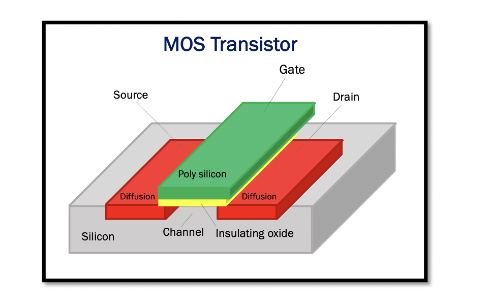
MOS refers to Metal-Oxide-Semiconductor, and MOSFET refers to Metal-Oxide-Semiconductor Field Effect Transistor. MOSFET has four terminals: drain, source, bulk, and gate. There are two types of MOSFET: NMOS type transistor and PMOS type transistor. The below figure shows the cross-section of the NMOS transistor. It includes the bulk, which is a p-type semiconductor, and the source and drain are n-type semiconductor.
Structure of NMOS
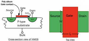
We know that a MOS structure is made up of a metal, oxide layer, and a substrate. The metal connects to the gate and is called the polysilicon gate contact. In between the gate and substrate, there is an insulator made up of silicon dioxide. In the MOS structure, the p-type substrate is diffused to form an n+ source and drain terminals. The region between the drain and source is called the channel. The top view of the NMOS shows the structure is symmetric concerning drain and source. ‘L’ is the length of the channel, and ‘W’ is the width. Based on the channel, there are two types of MOS transistors, enhancement type, and depletion type. When the gate voltage is 0 (VGS=0), there is no conducting channel in enhancement type. Hence, we can say the device is in an off mode at zero gate voltage. In depletion type, when VGS = 0, there is conducting channel between the source and drain.
Conduction between source and drain
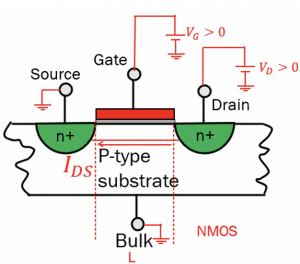
The source and bulk are grounded, and the drain is connected to a positive voltage (VD). The electrons flow from the source terminal to drain as the drain has a positive voltage, and the direction of current is the opposite of the flow of electrons. Therefore the flow of current (IDS) is from drain to source. This forms a channel between the source and drain.
In an NMOS type transistor, the electrons are the current carriers, so if there is positive voltage, it attracts the negative electrons to the channels to conduct. In a PMOS type transistor, the current carriers are holes, so if the voltage is negative, it attracts the positive holes to the channel to conduct. On the contrary, if a negative voltage is applied to NMOS and a positive voltage is applied to PMOS, it counters the free carriers, so there is no flow, and hence the device doesn’t conduct.
Structure of PMOS
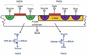
PMOS can be made by having N-well inside the p-type substrate. Symbols to represent NMOS and PMOS: when the arrow is pointed towards the source, it represents NMOS, and when it is pointed inwards to the transistor, it represents PMOS.
 NMOS curves
 Case 1: When VDS is constant
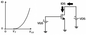
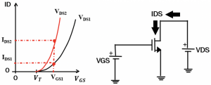
In the circuit above, the transistor is connected to the gate voltage VGS. The drain is connected to voltage VDS, and the source is grounded. Let VDS be a constant non-zero value. When the transistor gate voltage increases from 0 and reaches a positive voltage up to a point called VTH (threshold voltage), the transistor is said to be turned on. The current (IDS) increases with an increase in gate voltage VGS, as represented in the graph.
Case 2: When VDS is not constant
When the drain voltage VDS increases to a higher value, VDS1 to VDS2, then as shown in the graph, VDS2 > VDS1, and the current also increases. For a constant gate voltage VGS1, if we increase drain voltage VDS, we will have a higher current value IDS2, where IDS2> IDS1.
Case 3: When VDS and VGS are changed at the same time
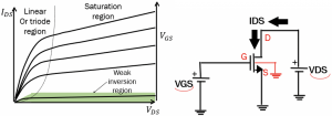
In this graph, the x-axis represents the increase of drain voltage VDS, and there are different curves for different gate voltage represented from VGS1 to VGS5. The VDS and VGS are changed simultaneously, and VGS5 will have the highest value, VGS5>…>VGS1.
Different regions in the NMOS curve
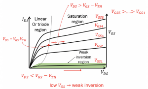
Assuming that the source voltage is constant, and the drain-source voltage increases from 0 to a positive value. The current increases linearly until the amount of current saturates. The region before saturation is called the Linear or triode region. In linear or triode region: VDS<VGS-VTH. If the gate voltage increases, you can see that the VDS gets higher with the more current flow until it reaches saturation. In the saturation region, the VDS increases, but the IDS doesn’t rise to a much higher value. Comparing different VGS, we see the greater VGS value yields a greater triode region before saturation. In Saturation region: VDS>VGS-VTH.
The weak inversion region is when the VDS is changing; however, the VGS remains very low. When there is low VGS, the transistor is said to be working in a weak inversion region. Sometimes the transistor works at very low voltage, even below the threshold voltage, and this region is the weak inversion region.
 Current Equations
Early voltage (VA)
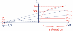
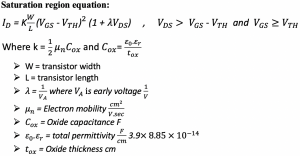
When the curves in the graphs are extended, they meet at a point in the negative region. This point is referred to as the Early voltage VA. In a long length channel where L is high, the VDS increases with constant gate voltage, and the IDS remains constant. If those curves are extended to point to the early voltage, we get a very high negative value. Since λ is the inverse of VA, in long length channel λ is very low, sometimes considered 0. Whereas in the short channel, the current changes in the saturation region and increases with VDS, the slope is higher, and the early voltage points at a smaller value. Therefore, λ for the short channel will be higher. As per the equation in saturation, when VDS increases, the ID also increases.
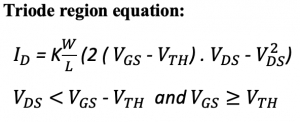
As discussed before that in the linear region, the curves depend on both VGS and VDS. All these equations are concerning NMOS. For PMOS equations, the VGS can be changed to VSG and VDS to VSD. For example, the PMOS triode region will be VSD<VSG-VTH.

Learn more about this topic by taking the complete course ‘’RF Design Theory and Principles – RAHRF201’’.
Watch the course videos for more detailed understanding. Also checkout other courses on RF system and IC design on https://rahsoft.com/courses/
Rahsoft also provides a certificate on Radio Frequency. All the courses offer step by step approach.
Tag:MOS Transistor, MOSFET, n-type, p-type, Semiconductor

