Small Signal Analysis of MOS Transistor
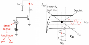
The operation point of the transistor is called biasing. Biasing is done before performing the small-signal analysis. To bias, the transistor, positive gate voltage is applied to the transistor. In this given circuit, VS is the small signal where the amplitude is low like 1mV. This circuit also shows a DC source. It has both AC and DC going into the gate of the transistor. There is load (RL) in the circuit connected to voltage VDD.
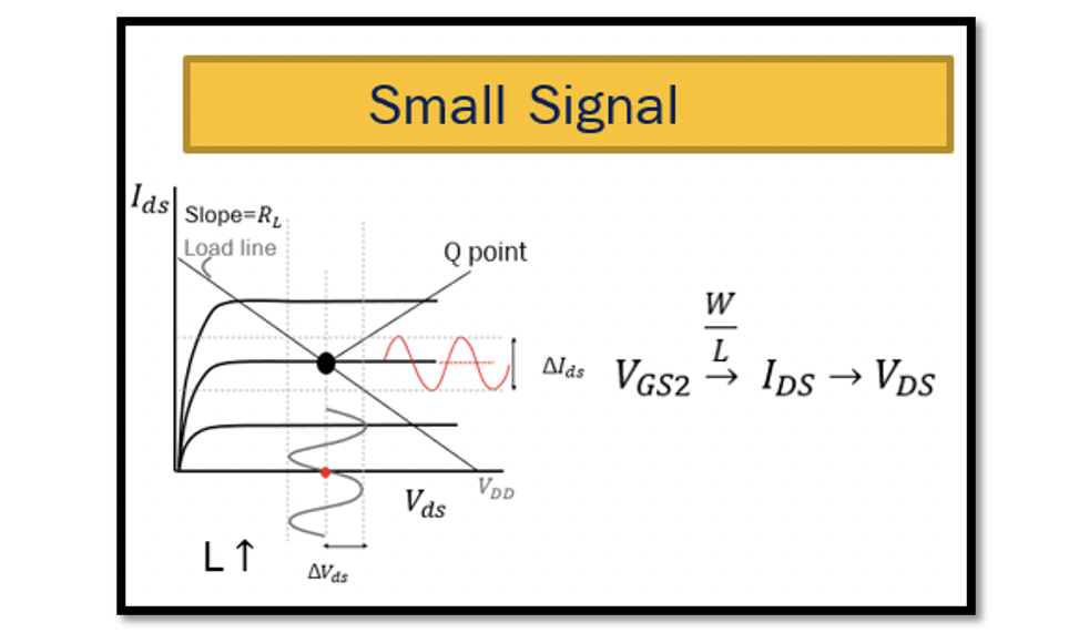
The operating point for the transistor is chosen using the shown graph. VGS is set for the transistor and changing the transistor size (W/L), we are getting the current IDS.
As read before from the Early Voltage section in the MOS transistor for long length channel, the curve slope is almost constant in the saturation region. When L is high, λ is very low, sometimes considered 0 in the saturation region equation.
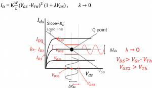
There are three curves in this graph representing VGS1, VGS2, and VGS3. Using these, we can get the drain-source voltage, VDS. Taking the reference of VGS2 in this case, the current is ID2 which is the DC point of our current as marked on the graph. Therefore, VDS can be calculated as VDS = VDD-RL.ID. Using this equation, the VDS is calculated and is the bias point. As we read before that, in saturation region VDS>VGS – VTH, therefore VGS should be more than VTH (VGS>VTH) for the transistor to turn on and work in the saturation region. Now we got the DC values.
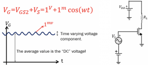
This figure shows the AC simulation. The transistor receives both AC & DC; shown in the circuit diagram, there is a DC source to provide the gate voltage. The DC voltage is VGS2. After reaching the Q point, the AC is applied. AC can be a cosine wave with low amplitude; for example, it is 1mV (should be more than the threshold voltage VTH). Hence, VG in total can be calculated as VG=VGS2+VS = 1V+1m cos(wt).

The signal provided to the gate and other parts of the transistor is alternating. The graph represents the fluctuations. The alternating current limits are shown in the axis for VGS2, the maximum value for this example can be 1V+1mV, and the minimum can be 1V-1mV. There is a small fluctuation in the drain current (IDS) which is a small signal. It fluctuates between ID1 & ID3; similarly, VDS is fluctuating between VDS1 and VDS3.
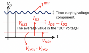
To represent other values like current, the DC value is ID2, and for voltage, it is VDS2, the amplitude for describing the current wave is ID3-ID2, and for VDS2, the amplitude 0f the wave will be VDS3-VDS2.
Defining the gm parameter
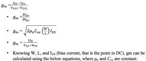
One of the important parameter for the transistor is gm, and it is equal to the fluctuation of current (IDS) to fluctuation of gate-source voltage (VGS).
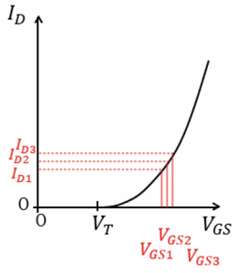
In the graph, the bias point VGS2 is plotted, for which the current bias is ID2. Now we know that VGS is a small signal and is changing. As shown in the graph, the fluctuation for ID2 has minimum values (IDS1 & VDS1) and maximum values (IDS3 & VDS3). The slope gm calculated for this portion will be equal to:
To summarise, in small-signal analysis, AC and DC voltage can be applied together to the gate of the transistor, and we can get the small signal for the varying current and varying drain voltage.

Learn more about this topic by taking the complete course ‘’RF Design Theory and Principles – RAHRF201’’.
Watch the course videos for more detailed understanding. Also checkout other courses on RF system and IC design on https://rahsoft.com/courses/
Rahsoft also provides a certificate on Radio Frequency. All the courses offer step by step approach.
You may also like
Understanding Quadrature Amplitude Modulation (QAM) and Its Applications