Parasitic Capacitances in MOS Transistor
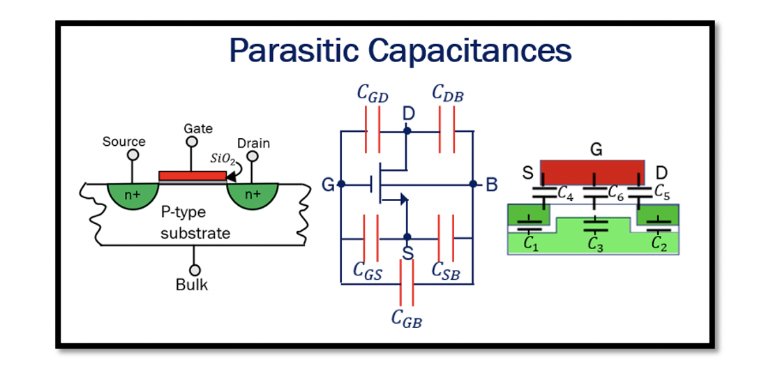
MOS Transistor parasitic capacitances are formed due to the separation of mobile charges at various regions within the structure. Parasitic Capacitances are the unwanted component in the circuit which are neglected while working in low-frequency. But cannot be avoided when working in high-frequency RF circuits; therefore, we have to be careful about parasitic capacitance while designing.
The impedance for capacitance is 1/jcw. For low frequency, it is considered infinity; hence it is open and doesn’t affect the circuit. However, when the frequency increases, the capacitance in the circuit behaves like an impedance, and it can change the behaviour of our transistor by limiting its speed. Hence, the transistor has limits while working with high frequencies.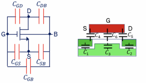
These capacitances are formed within the transistor due to its arrangement. As you can see from the transistor’s cross-section, the C1 capacitance is formed due to the depletion regions—the depletion region around forms separation between bulk and source. In the same way, there is capacitance C2 due to separation between bulk and drain. As there is an n-type and p-type semiconductor, they are the depletion capacitances. These depletion capacitances are a drain to bulk CDB and source to bulk CSB.
Take our entry level course (Below) for free using coupon code RAHRF101BLOG
RF Fundamentals, Basic Concepts and Components – RAHRF101
For limited time take an additional 10% off of all our courses using coupon code RFCERT10
Rahsoft RF Certificate and courses
Looking closely into the MOSFET structure, we could see an overlap at the gate metal oxide and source region edges. When voltage Vgs is applied, charges get accumulated at this region, forming a capacitance (C4/CGS), similar to the parallel plate capacitor where the lower plate is source region n+ type (NMOS) and the upper plate is metal. Similarly, a capacitance (C5/CGD) is formed between gate metal oxide and drain region. They are called overlap capacitance. C3 & C6 are formed between the gate and substrate. The capacitance that is from channel to bulk depends on the state of the substrate. The capacitance from gate to bulk C6, there is an oxide layer as we know. This capacitance can be between gate and channel and between channel and bulk (C3). CGB represents this capacitance.
As read before in brief review of MOSFET Structure, there are three regions in which the transistor works: off, triode, and saturation region. Mostly we work in the saturation region. In the Saturation region, the gate-source capacitance CGS can be calculated using the below equation:
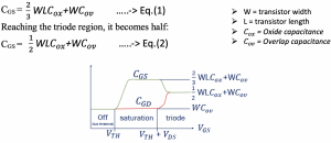
In the saturation region, the highest capacitance in our circuit is CGS. The input capacitance to the transistor gate is equal to Cin=CGS, and working in the saturation region, and the value can be calculated using equation (1). CGS has a higher value compared to the gate-drain capacitance CGD, which is equal to WCov.

This circuit diagram shows a high-frequency small-signal model similar to that shown in the small signal model of MOSFET. The model becomes a bit complicated in high-frequency.
Due to the effect of bulk, this circuit has gmbvbs. However, gmb <<gm; hence it is ignored sometimes. In high-frequency models, the capacitance becomes dominant. The two important capacitance that is taken into account are CGS & CGD
The parasitic capacitance limits the speed of our circuit. Changing the transistor size affects the speed. Hence, while making design choices, the circuit designers have to consider how the options made affect the circuit’s speed. The speed of the MOS Transistor is measured by unity-gain frequency fT. As shown in the circuit diagram, fT is when the current enters the gate iin equals the current flow through channel iout. We can also say that fT is a frequency at which the current gain becomes 1.
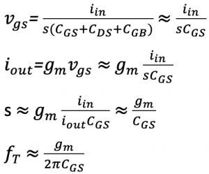
From the above equation, the fT depends on gm and CGS. If there is high transconductance (gm), there will be a high-speed transistor. To get a high gm, the current should be increased, as per the equation:
![]()
So the trade-off is; if we have a high current, then there will be high power. Another trade-off as per equation (1) is that the CGS has to be decreased, but doing that, the size of the transistor also decreases. Since CGS as per equation (1) depends on W/L.
The dimensions of the transistor control the capacitance CGS. Hence, a small-size transistor must operate at high power; however, a small-size transistor will result in a weak inversion region and not in the saturation region. Therefore, an effective circuit designer needs to make a good trade-off by understanding the choices.

To have a high-speed transistor, the power has to be increased. As we can see fT for low frequency, the current gain is high, but the frequency increases it falls, reaching fT to 1. The fT affects gain. We know that gain=gm(RL||r0) is DC gain and it is in low frequency from the small-signal model analysis. This model works on low frequency, and parasitic capacitance is not taken into account. In the high-frequency model, if we calculate the gain, there is capacitance in the equation. By increasing frequency, the gain will decrease until it reaches 1. So the designers have to choose the region so that the transistor’s gain is not very low by increasing the power and adjusting the dimensions of the transistor.


