Bias Networks for Low Noise Amplifiers (LNAs) Using Microstrip Transmission Lines
Introduction
Low Noise Amplifiers (LNAs) are crucial components in RF and microwave systems, primarily used to amplify weak signals without significantly degrading the signal-to-noise ratio (SNR). One of the key challenges in LNA design is ensuring proper biasing of the active device (usually a transistor) while maintaining excellent RF performance. In this blog, we will delve into the role of bias networks in LNA design using microstrip transmission lines, exploring the principles, components, calculations, and design considerations.
Understanding Bias Networks
Bias networks serve two primary functions in LNA design:
- Establishing the DC Operating Point: They provide the necessary DC voltage and current to set the transistor’s operating point.
- Ensuring RF Performance: They must isolate the DC biasing from the RF signals, preventing any adverse effects on the signal integrity and overall performance of the LNA.
Components of Bias Networks
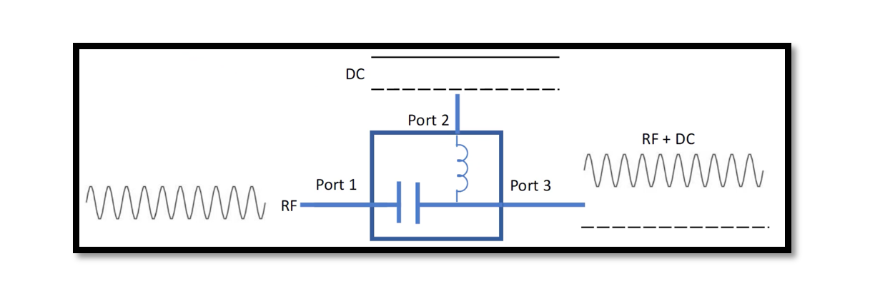
- Bias Tees: Combine DC and RF signals using an inductor to block RF from the DC supply and a capacitor to block DC from the RF path.
- Decoupling Capacitors: Filter out RF signals from the DC supply lines.
- RF Chokes (Inductors): Block RF signals from entering the DC bias network.
- Resistors: Set the correct DC operating point and can be used in feedback networks.
Design Considerations
- Impedance Matching: Ensuring minimal disturbance to the RF signal path.
- Isolation: Preventing RF signals from affecting the DC supply.
- Bypassing and Filtering: Using capacitors to ensure RF does not appear on the DC lines.
- Thermal Stability: Maintaining a stable operating point over temperature variations.
Example Design Process
Let’s consider a typical LNA design using a GaAs FET as the active device. We’ll focus on the bias networks for the gate and drain of the FET.
Step 1: Determine Bias Points
For a given FET, assume we have the following desired bias points:
- Gate Voltage (V_G): -0.5V
- Drain Voltage (V_D): 3V
- Drain Current (I_D): 10 mA
Step 2: Bias Network for Gate
The gate bias network needs to provide -0.5V to the gate while blocking RF signals.
Components:
- Bias Resistor (R_G): Sets the gate voltage.
- RF Choke (L_G): Blocks RF signals.
- Decoupling Capacitor (C_G): Filters out RF signals from the bias network.
Calculations:
- Choose RG to set the gate voltage. Since the gate current (I_G) is typically negligible, VG=−0.5V.
- 𝐿𝐺LG should have a high impedance at the operating frequency (f_0). Impedance of an inductor ZL=jωL, where ω=2πf0.

Microstrip Implementation:
- Use a high-impedance microstrip line (narrow width) to implement LG.
- Place CG close to the gate to bypass RF to ground.
Step 3: Bias Network for Drain
The drain bias network needs to supply 3V to the drain while isolating RF signals.
Components:
- RF Choke (L_D): Blocks RF signals.
- Decoupling Capacitor (C_D): Filters out RF signals from the bias network.
Calculations:
- Choose LD to block RF signals. Again, use ZL=jωL.

Microstrip Implementation:
- Use a high-impedance microstrip line to implement LD.
- Place CD close to the drain to bypass RF to ground.
Take our entry level course (Below) for free using coupon code RAHRF101BLOG
RF Fundamentals, Basic Concepts and Components – RAHRF101
For limited time take an additional 10% off of all our courses using coupon code RFCERT10
Rahsoft RF Certificate and courses
Example Configuration and Design
Schematic Overview
- Input Network: RF signal to the gate through a matching network and coupling capacitor.
- Gate Bias Network: High-impedance microstrip line for RF choke, decoupling capacitor to ground.
- Drain Bias Network: High-impedance microstrip line for RF choke, decoupling capacitor to ground.
- Output Network: Amplified signal from the drain through a matching network and DC blocking capacitor.
Implementation Steps
- Microstrip Line Design:
- Calculate the characteristic impedance Z0 and effective dielectric constant ϵeff for the microstrip lines.
- Use microstrip design equations or software tools for precise layout.
- Component Selection:
- Choose capacitors with low ESR and high self-resonance frequency.
- Ensure inductors have a high Q factor at the operating frequency.
- Simulation and Optimization:
- Simulate the LNA circuit using software like ADS or HFSS.
- Optimize the layout for minimal insertion loss and reflection.
Conclusion
Designing bias networks for LNAs using microstrip transmission lines involves a careful balance between providing the necessary DC operating points and ensuring minimal impact on the RF performance. By strategically placing inductors and capacitors, and using high-impedance microstrip lines, designers can achieve effective biasing while maintaining excellent signal integrity. Through detailed calculations and thoughtful component selection, robust and high-performing LNA designs can be realized, enhancing the performance of RF and microwave systems.

Learn more about this topic by taking the complete course ‘Microwave Amplifier and Low Noise Amplifier (LNA) Design Theory and Principles online course – RAHRF526’. Watch the course videos for more detailed understanding. Also checkout other courses on RF system and IC design on https://rahsoft.com/courses/. Rahsoft also provides a certificate on Radio Frequency. All the courses offer step by step approach.


