Phase-Noise contributors in a PLL circuit – Part 1
In this blog, we will explore individual Phase-Nosie contributors in a Phase-Locked Loop, how they get shaped by closed loop, and how they combine to produce typical Phase-Noise profile of a PLL. This fundamental understanding is vital in optimizing Phase-Noise performance of overall RF-systems. Before proceeding to the further discussion, you are encouraged to learn the un-wanted effects of phase-noise on RF system’s performance, read this blog: How Phase-Noise affects RF System Performance?
In the following, a typical Phase-locked loop has been shown that employs following building blocks:
- VCO as a high-frequency oscillator. The principal objective of PLL circuit is to lock the phase of high-frequency VCO to a stable low-frequency REF clock.
- Phase detector (PD) compares the phase of REF clock with that of VCO
- Charge Pump (CP) creates current pulses on the basis of phase difference between REF clock and VCO.
- Loop Filter is a low-pass filter that smooths the current pulses and creates a ripple free voltage signal, which acts as Control voltage for VCO.
- N-divider is a frequency divider that brings down VCO frequency to REF Clock frequency. This way loop is closed forming a negative-feedback control system.
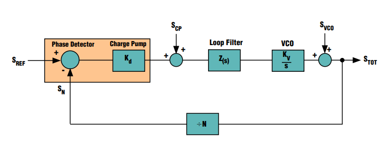
In above diagram, we can define:
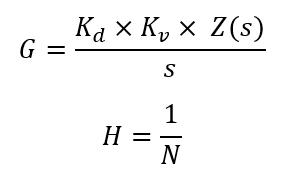
Individual noise contributors in above PLL circuit are as follows:
- SREF is the noise voltage – available on positive input of PD – which depends upon Reference divider/doubler circuitry and the Phase-noise characteristics of REF clock itself.
- SN is the noise voltage – available on negative input of PD – which depends upon feedback divider-N circuitry.
- SCP is the noise voltage added by PD and Charge-pump circuitry.
- SVCO is the noise voltage added by VCO itself. Its profile is well-defined by modified Leeson’s Oscillator phase-noise model.
Total phase-noise of the PLL circuit is the rms addition of above-mentioned components such that
STOT = X2 + Y2 + Z2
where:
- STOT is the total Phase-noise power at the output
- X2 is the noise power due to SREF and SN
- Y2 is the noise power due to SCP
- Z2 is the noise power due to SVCO
In the following, we will discuss how individual contributors’ Phase-noise gets shaped by closed-loop to form overall phase-noise profile of PLL circuit.
(1) REF clock and N-divider contributions are dominant within loop-bandwidth only as they are low-pass filtered by closed loop. These contributions can be minimized by reducing N value.
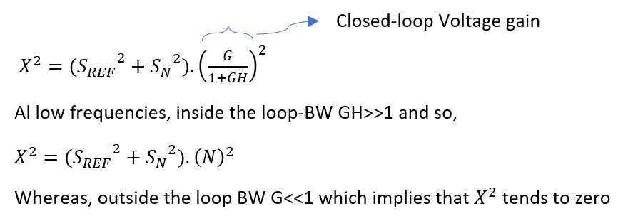
Above equations clearly describe that we can choose higher REF clock (PFD frequency) to reduce the N value and improve close-in phase-noise, associated with REF clock, at PLL output.
(2) Phase-Detector and charge-pump (PLL-noise) contributions are also dominant within loop bandwidth only and low-pass filtered by closed-loop. These can be minimized by increasing charge-pump current. First off, we can refer SCP at the PD input and then calculate its overall contribution at PLL output by multiplying input-referred SCP by closed-loop gain

Using the similar argument that GH>>1 inside loop bandwidth and G<<1 outside the loop bandwidth, it is claimed that PD and CP phase noise is low-pass filtered by closed loop. Above equation clearly shows that if we optimally increase charge-pump current (by increasing Kd), the in-band phase-noise contributions due to PD and CP can be reduced at PLL output.
The PD and CP contributions along with N-divider’s phase-noise can be termed as PLL-noise, and it has two regions: (a) PLL flicker (1/f) noise and (b) PLL flat noise. How these two regions relate to N value and PFD frequency, we will discuss in a separate blog as it requires detailed discussion. Just to mention briefly, PLL flicker noise is independent of PFD frequency, whereas PLL flat noise can be improved by using higher PFD frequency (and lower N value).
(3) VCO Phase-Noise is high-pass filtered by closed loop and so, it gets suppressed within loop bandwidth and dominate overall PLL phase-noise profile outside the loop bandwidth only. Now, the forward gain is simply 1, whereas the gain for feedback signal remains the same. So, the transfer function reduces to:
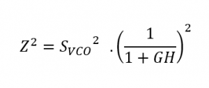
Since, G is a low-pass response as defined in the start of the post, VCO noise is high-pass filtered and governs overall phase-noise profile outside the loop bandwidth only.
So far, we have mathematically established the shaping of individual phase-noise contributors by closed loop. In next blog, we will present pictorial explanations to this concept along with design example. Moreover, detailed discussions on PLL-noise part will also be presented in coming blogs.

Learn more about this topic by taking the complete course ‘RF System Design of Receivers, Transmitters & Transceivers – RAHRF409’. Watch the course videos for more detailed understanding. Also checkout other courses on RF system and IC design on https://rahsoft.com/courses/. Rahsoft also provides a certificate on Radio Frequency. All the courses offer step by step approach.
Tag:Phase Noise, PLL

