Concept of Small Signal Model of MOSFET
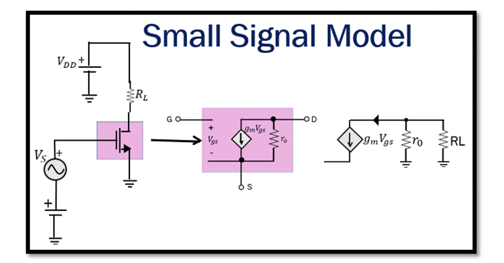
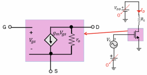
In this circuit, the Vgs is the input signal applied between gate and source terminal, and we know that the change in drain current is linearly proportional to Vgs. In this model, if you consider the effect of channel and modulation, then there will also be an output resistance (r0). If it is for a long length channel, then, as read in the Early Voltage section in the MOS transistor for a long length channel, the curve slope is almost constant in the saturation region, λ is very low, sometimes considered 0. Therefore, under the small-signal approximation, the MOS transistor can be replaced by the small-signal model.
Take our entry level course (Below) for free using coupon code RAHRF101BLOG
RF Fundamentals, Basic Concepts and Components – RAHRF101
For limited time take an additional 10% off of all our courses using coupon code RFCERT10
Rahsoft RF Certificate and courses
In the small-signal model, there is an output resistance r0 and the current source is gmVgs, so if we can find the Transconductance (gm), we can find the value of current in this circuit. Output resistance r0 is the fluctuation of drain-source voltage to current. For the long channel transistor, the VA (early voltage) is high, and as per the equation, r0 is directly proportional to length; therefore, r0 is high for the long channel transistor. Here, ID is the current bias.
![]()
While doing the AC analysis, all the DC voltage in the circuit is assumed 0 and vice versa. The analysis for DC and AC is done separately. When we talk about gain, it is AC gain, and DC is just to set the operation point. So as you see, when the small circuit model is replaced for the transistor, we get the below circuit arrangement:

AC analysis for the given circuit considering DC is 0 & VDD is grounded. VS in a small signal model is placed between gate and source terminal. When input signal VS is very low, the MOS transistor can be replaced by the small-signal model. The flow of current is clockwise and is gmVGS, and V0 is connected to load resistance RL. R0 and RL are in a parallel arrangement. Therefore, gain here will be gmVGS. (RL||r0) and this value is more than 1, and this shows that the output voltage will be amplified.

The transistor in this model works as an amplifier. If VS is 1mV AC and good gain, then output from point V0 can be up to 10mV. The work is mostly in the saturation region due to the reason of having high output resistance. The small-signal model of the MOS transistor is useful as an amplifier. It is easy to analyze the circuits using small-signal models.
In summary, so far, we have read that using the MOS Transistor as an amplifier should be operated in the saturation region. In this region, the transistor acts as a voltage-controlled current source, and the drain current is a function of Vgs. The relationship between the VGS and drain current is non-linear.
For a set Vgs, the amount of change in the drain current is dependent on the bias point, and it is defined as the Transconductance of the MOS transistor. If the biasing point changes, then for the same change in the Vgs, there will be more change in the drain current ID. As we read from the small signal analysis the Transconductance is equal to change in the drain current to change in Vgs. For a given change in Vgs, the difference in the drain current graphically is the slope of the curve at the operating point.
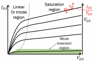
In the graph, you see that the slope of the curve is very low, it is equal to IDS/VDS, which is the inverse of r0 from equation (1). Hence, when the slope is high, r0 is low, and vice versa. In the saturation region, the output resistance of the transistor is increased as the slope is low, and resistance is much higher for a long length channel. In linear regions, the slope is more, and hence the output resistance is less. Mostly the work done in the transistor is in the saturation region as we have higher output resistance.


