
Please Note Pre-Requisites for this course are:
| RF Design Theory and Principles | RAHRF201 |
| Keysight Advanced Design System (ADS) Basics and Applications | RAHRF209L |
| Microwave Amplifier and Low Noise Amplifier (LNA) Design Theory and Principles | RAHRF526 |
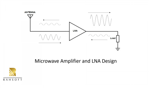
Course Title: RF IC Design – Low Noise Amplifiers (LNA) Simulation – RAHRF527
Course Description: Welcome to RAHRF527, an advanced online course that delves deep into the realm of Low Noise Amplifier (LNA) simulation for RF IC Design. This course assumes a strong foundation in RF Design Theory and Principles, Keysight Advanced Design System (ADS) Basics and Applications, and Microwave Amplifier and Low Noise Amplifier (LNA) Design Theory and Principles.
Course Prerequisites:
- RF Design Theory and Principles (RAHRF201)
- Keysight Advanced Design System (ADS) Basics and Applications (RAHRF209L)
- Microwave Amplifier and Low Noise Amplifier (LNA) Design Theory and Principles (RAHRF526)
Course Overview: RAHRF527 is an advanced course that will empower you with the knowledge and skills to simulate and optimize various LNA topologies. In this comprehensive course, you’ll explore the following key topics:
7.1 BASIC RAHSOFT RF CERTIFICATE INTRODUCTION (3 Lectures):
- Gain insights into the Rahsoft RF Certificate program.
- Discover the course objectives and expectations.
7.2 RF IC LNA FUNDAMENTALS (9 Lectures):
- Learn the fundamentals of Low Noise Amplifiers (LNAs).
- Explore different LNA topologies, including CMOS LNAs.
- Understand critical aspects such as noise figure, gain, and bandwidth.
7.3 LNA RF IC DESIGN (8 Lectures):
- Dive into the detailed simulation of a Single Stage Common Source Narrow Band LNA IC at 1GHz.
- Step-by-step guidance on LNA design and simulation using ADS.
7.4 SIMULATION OF SINGLE STAGE SOURCE DEGENERATED CASCODE LNA (7 Lectures):
- Explore the simulation of a Single Stage Source Degenerated Cascode LNA.
- Analyze the pros and cons, biasing, transistor sizing, matching, and more.
7.4 LNA IC LAYOUT GUIDE (SUBSECTION) (6 Lectures):
- Delve into the crucial aspects of LNA IC layout, including pad frame, routing, metal mesh, and Mos-Cap.
- Master the art of layout design for a Cascode LNA.
7.5 ANALYSIS OF COMMON GATE LNA (4 Lectures):
- Analyze the Common Gate LNA, covering input matching, voltage gain, noise figure, and finite drain-source resistance issues.
- Compare Common Gate and Common Source LNAs.
7.6 DESIGN OF WIDEBAND LNA 3-7GHZ (5 Lectures):
- Explore the techniques behind Wideband LNA design.
- Step through the design process for the 1st and 2nd stages of a Wideband LNA.
Who Should Enroll: This course is tailored for professionals, engineers, and students who have completed the prerequisite courses and are eager to excel in RF IC Design with a focus on LNA simulation. If you aspire to become an RF IC design expert, this course is your gateway to success.
Please Note:
- This course is highly advanced and builds upon prior knowledge of RF fundamentals.
- Extensive hands-on simulation and optimization exercises are included.
- Master the art of LNA IC design and layout through comprehensive learning modules.
Join us in RAHRF527 and elevate your RF IC Design skills to a level where you can confidently design and simulate Low Noise Amplifiers for various applications in the RF domain.
Course Features
- Lectures 42
- Quiz 0
- Duration 9 hours 47 minutes
- Skill level All levels
- Language English
- Students 331
- Certificate Yes
- Assessments Yes
Curriculum
- 7 Sections
- 42 Lessons
- 900 Weeks
- 7.1 Basic Rahsoft RF Certificate IntroductionBasic Rahsoft RF Certificate Introduction3
- 7.2 RF IC LNA fundamentals9
- 2.17.1.0.0 Design and Simulation of Low Noise Amplifier Topologies15 Minutes
- 2.27.2.1.1 CMOS Low Noise Amplifier Topologies19 Minutes
- 2.37.2.1.2 Common source CMOS LNA with reduced NF17 Minutes
- 2.47.2.2.1 Source Degenerated Common Source CMOS LNA21 Minutes
- 2.57.2.2.2 Source Degenerated Common Source CMOS LNA Load10 Minutes
- 2.67.2.2.3 Source Degenerated Common Source CMOS LNA Bandwidth adn Gain10 Minutes
- 2.77.2.2.4 Source Degenerated Common Source CMOS LNA Av=Gain?13 Minutes
- 2.87.2.2.5 Source Degenerated Common Source CMOS LNA NF – Noise Figure / Factor25 Minutes
- 2.97.2.2.6 Source Degenerated Common Source CMOS LNA NF Example and trade off between matching and NF14 Minutes
- 7.3 LNA RF IC Design: Simulation of Single Stage Common Source Narrow band LNA IC @ 1GHzIn this section we will be going over different typologies and design different LNA RF ICs mainly Simulation of Single Stage Common Source Narrow band LNA IC @ 1GHz8
- 3.17.3.1.1 Design of complete single stage low noise amplifier Step by Step Simulation using ADS Part 126 Minutes
- 3.27.3.1.2 Design of complete single stage low noise amplifier Step by Step Simulation using ADS Part 213 Minutes
- 3.37.3.1.3 Design of complete single stage low noise amplifier Step by Step Simulation using ADS Part 321 Minutes
- 3.47.3.1.4 Design of complete single stage low noise amplifier Step by Step Simulation using ADS Part 420 Minutes
- 3.57.3.1.5 Design of complete single stage low noise amplifier Step by Step Simulation using ADS Part 512 Minutes
- 3.67.3.1.6 Design of complete single stage low noise amplifier Step by Step Simulation using ADS Part 613 Minutes
- 3.77.3.1.7 Single stage Common Source – Final Optimization9 Minutes
- 3.87.3.1.8 Single stage Common Source – Compression point simulation16 Minutes
- 7.4 Simulation of Single Stage Source Degenerated Cascode LNA @ 2.4GHzIn this section we will be going over different typologies and design different LNA RF ICs mainly Simulation of Single Stage Source Degenerated Cascode LNA7
- 4.17.4.1.1 Single Stage Source Degenerated LNA – Pros and Cons9 Minutes
- 4.27.4.1.2 Single Stage Source Degenerated LNA – Biasing14 Minutes
- 4.37.4.1.3 Single Stage Source Degenerated LNA – Transistor size and input impedance18 Minutes
- 4.47.4.1.4 Single Stage Source Degenerated LNA – Matching20 Minutes
- 4.57.4.1.5 Bond-wire and Packing effect on Design17 Minutes
- 4.67.4.1.6 Single Stage Source Degenerated LNA – IIP3 simulation8 Minutes
- 4.77.4 Course Project video5 Minutes
- 7.4 LNA IC Layout Guide (subsection)6
- 5.17.4.2.1 Pad frame and Routing15 Minutes
- 5.27.4.2.2 Metal Mesh and Mos-Cap16 Minutes
- 5.37.4.2.3 Layout Design for Cascode LNA part 119 Minutes
- 5.47.4.2.4 Layout Design for Cascode LNA part 211 Minutes
- 5.57.4.2.5 Layout Design for Cascode LNA part 37 Minutes
- 5.67.4.2.6 Layout Design for Cascode LNA part 411 Minutes
- 7.5 Analysis of Common Gate LNA4
- 7.6 Design of Wideband LNA 3-7GHz5
- 7.17.6.1.1 Wide band LNA Design Technique14 Minutes
- 7.27.6.1.2 Wide band LNA Design – 1st Stage18 Minutes
- 7.37.6.1.3 Wide band LNA Design – 2nd Stage23 Minutes
- 7.47.6.2.1 Wide band LNA Design Common Source input stage part113 Minutes
- 7.57.6.2.2 Wide band LNA Design Common Source input stage part216 Minutes